SAPI Host Interfaces#
The RS9116 WiSeConnect device supports SPI, UART and SDIO interfaces. This section describes the serial interfaces supported by WiSeConnect for the RS9116 device including features, protocols, and commands.
Serial Interfaces available include:
SPI Interface#
This section describes the RS9116 SPI interface and includes the commands and processes to operate the device via SPI.
Features#
The features are as follows:
8-bit and 32-bit data mode
Flow control
Hardware Interface#
The SPI interface on the RS9116-WiSeConnect works in secondary mode. It is a 4-wire interface. In addition to the SPI interface, the device provides an additional interrupt pin to signal events to the host. The interrupt is raised by the device in SPI mode for the following condition. When the device has data in its output buffer, it indicates host by raising the active high signal on the interrupt pin.
The interrupt from the device is active high, which means that the host has to configure the interrupt in level trigger mode. The RS9116W also supports edge-triggered interrupts, provided the host is configured to handle these appropriately. Note that this is generic and does not entail any specific implementation. The host must check for pending interrupts before clearing/acknowledging an interrupt to avoid missing interrupts and data.
Note! By default, the interrupt from the device is active high, however it can be configured active low in the bootloader menu.
SPI Signals#
SPI Interface is a full duplex serial Host interface, which supports 8-bit and 32-bit data mode. The SPI interface of the device consists of the following signals:
SPI_MOSI (Input) - Serial data input for the device.
SPI_MISO (Output) - Serial data output for the device.
SPI_CS (Input) - Active low secondary select signal. This should be low when SPI transactions are to be carried out.
SPI_CLK (Input) - SPI clock. The maximum value allowed is 80 MHz.
INTR (Output) - Active high (Default), Active low, level interrupt output from the device.
The device acts as an SPI secondary only, while the Host is the SPI main. Following parameters should be in the host SPI interface.
CPOL (clock polarity) = 0,
CPHA (clock phase) = 0.
Interrupt#
The device's INTERRUPT output signal should be connected to the interrupt input of the Host MCU. The INTERRUPT signal is an active high and level triggered signal. It is raised by the device in the following cases:
When the device needs to indicate to the Host that it has received data from the remote terminal and the data needs to be read by the Host.
When the device needs to indicate to the Host that a response to a command sent by the Host is ready to be read from the device.
To indicate to the Host that it should read a CARD READY message from the device. This operation is described in the subsequent sections.
An interrupt will be raised for asynchronous RX packets also.
SPI Interface Initialization#
This section explains the initialization of the SPI secondary interface in the device. These are the SPI initialization steps:
A host sends 0x00124A5C to the device.
On successful initialization, the device sends 0x58 (SPI success) to the host or the device sends 0x54 (SPI busy) or 0x52 (SPI failure).
Operations through SPI#
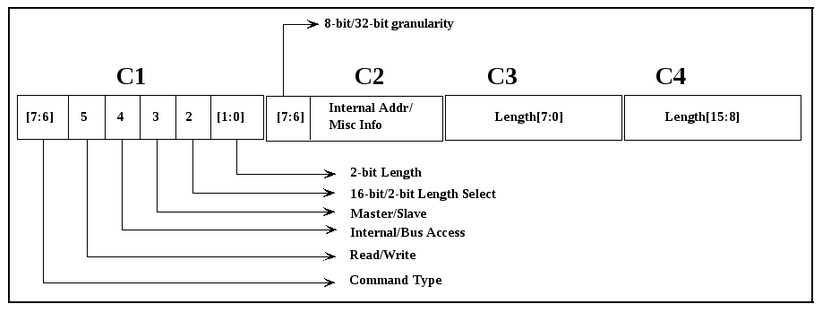
RS9116-WiSeConnect can be configured and operated from the Host by sending commands through the SPI interface. The SPI interface is programmed to perform a transfer using commands C1, C2, C3 and C4 and an optional 32-bit address. For all Commands and Addresses, the Host is configured to transmit data with the 8-bit mode. At the end of all the Commands and Addresses, the Host is reconfigured to transmit data with 8-bit or 32-bit mode depending on the commands issued. The Device responds to all the commands with a certain response pattern. C1, C2, C3, and C4 commands indicate to the SPI interface for all the aspects of the transfer. The command descriptions are as follows:
The SPI interface responds with a set of unique responses.
SPI Response#
RS9116 WiSeConnect gives responses to the host SPI command requests through the SPI interface, as follows:
A success/failure response at the end of receiving the command. This response is driven with 8-bit mode during the Command and Address phase and is then switched to 8-bit or 32-bit mode during the Data phase as per the command issued.
Success:
0x58Failure:
0x52
An 8-bit or 32-bit start token is transmitted after the four commands (C1, C2, C3, C4) indicating a read request are received and the Device is ready to transmit data. The start token is immediately followed by the read data.
Start Token:
0x55
An 8-bit or 32-bit busy response is initiated for a new transaction while the previous transaction is still pending from the secondary side.
Busy Response:
0x54
Bit Ordering of SPI Transactions#
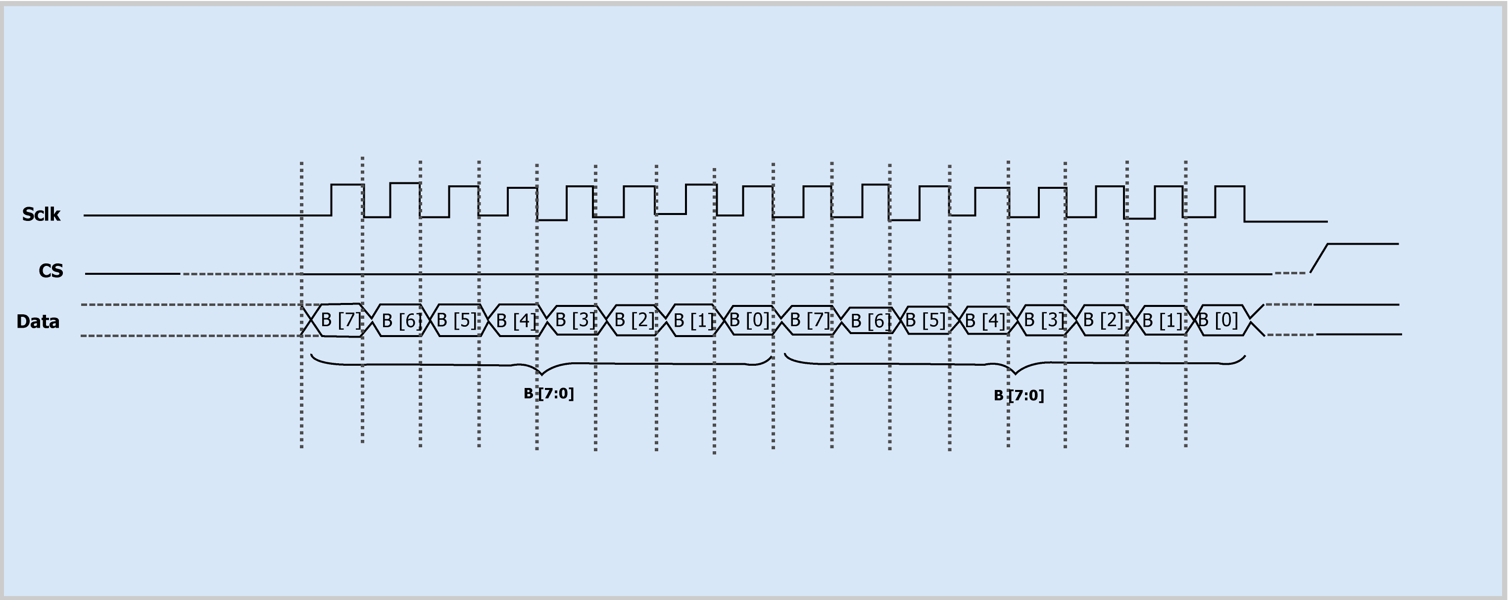
8-bit Mode#
For a sequence of bytes <B3[7:0]> <B2[7:0]> <B1[7:0]> <B0[7:0]> where B3 is interpreted as the most significant byte, the sequence of transmission is as follows:
B0[7] B0[6] .. B0[0] -> B1[7] B1[6] .. B1[0] -> B2[7] B2[6] .. B2[0] -> B3[7] B3[6] .. B3[0]
B0 is sent first, then B1, then B2, and so on. In each of the bytes, the MSB is sent first. For example, when B0 is sent, B0[7] is sent first, then B0[6], then B0[5], and so on. The same principle is true while receiving data. In this example, B0[7] is expected first by the receiver, then B0[6], and so on. Also, data changes value at the falling edge and is latched at the rising edge, as shown in the image below
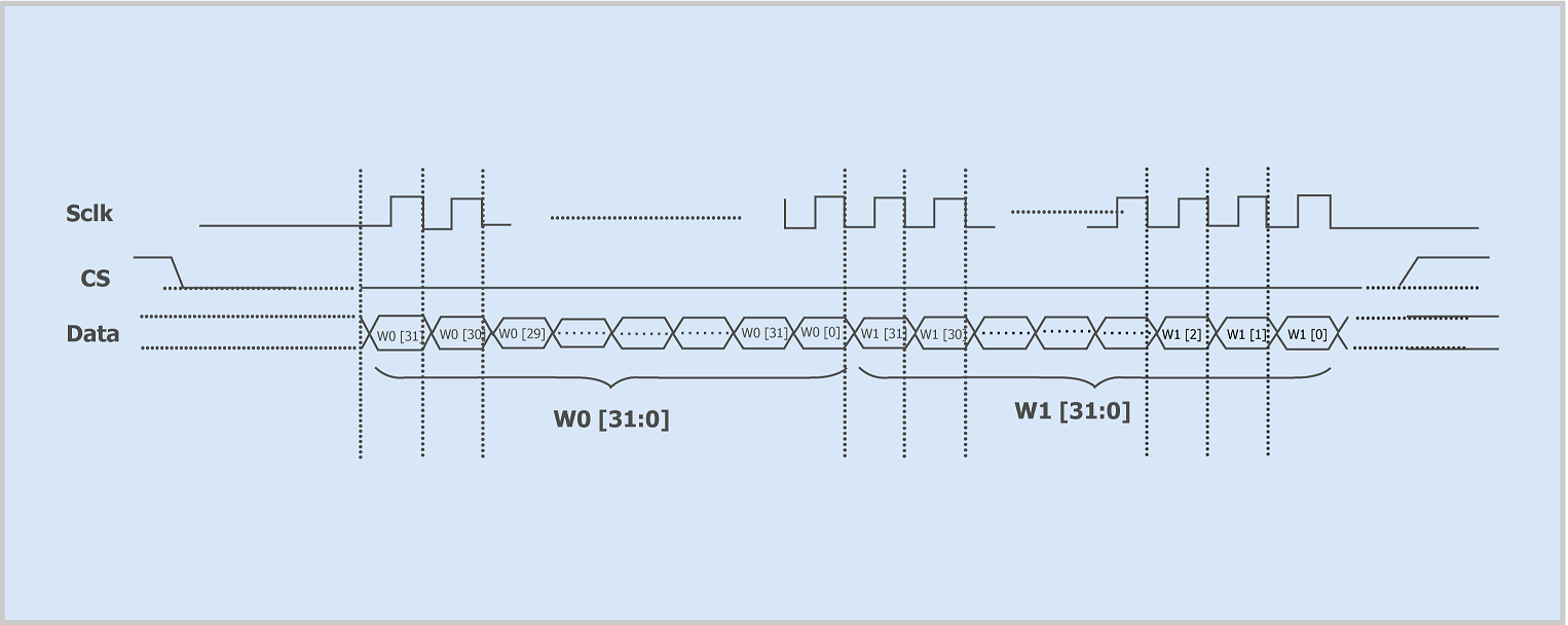
32-bit Mode#
For a sequence of 32-bit words <W3[31:0]> <W2[31:0]> <W1[31:0]> <W0[31:0]> where W3 is interpreted as the most significant word, the sequence of transmission is as follows:
W0[31] W0[30] .. W0[0] -> W1[31] W1[30] .. W1[0] -> W2[31] W2[30] .. W2[0] -> W3[31] W3[30] ..W3[0]
W0 is sent first, then W1, then W2, and so on. In each of the 32-bit words, the MSB is sent first. For example, when W0 is sent, W0[31] is sent first, then W0[30], then W0[29], and so on. The same principle is true when receiving data. In this example, W0[31] is expected first by the receiver, then W0[30], and so on. Also, data changes value at the falling edge and is latched at the rising edge, as shown in the image below.
Bit Ordering of SPI Response#
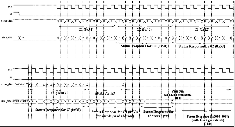
The bit ordering is same as explained in Device bit Ordering of SPI Transmission/Reception. For example, a 0x58 response for 8-bit success is sent as 0->1->0->1->1->0->0->0. That is, 0 is sent first, then 1, then 0, then 1, and so on.
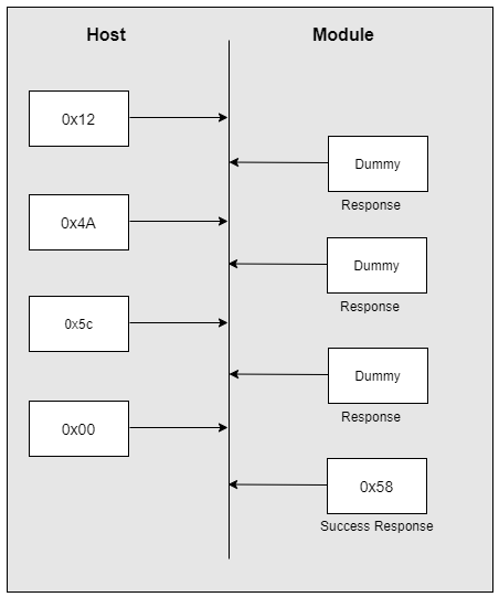
Device SPI Interface Initialization#
The Initialization command is given to the device to initialize the SPI interface. The SPI interface remains nonfunctional to all commands before initialization and responds only after successful initialization. Initialization should be done only once after the power is on. The device treats the subsequent initialization of any command before it is reset as an error. SPI initialization is a 24-bit command (0x124A5C) followed by 8 bits of dummy data. The 24-bit SPI Initialization command should be sent in a sequence of 0x12, 0x4A, 0x5C bytes. The status response from the SPI Interface is driven during the transmission of the dummy data i.e., after the transfer of 8-bits of command C1.
Host Interactions Using SPI Command#
This section describes procedures for the Host to interact with the RS9116 WiSeConnect using SPI commands. The Host interactions to the device can be categorized as shown in the following table.
Command | Bit Number | Description |
|---|---|---|
|
| Command Type. Initialization = |
| Read/Write. Read = | |
| Register/(Memory/Frame) R/W Access. Register R/W = | |
| Memory/Frame Access. Memory R/W = | |
| 2-bit or 16-bit transfer length. 2-bit length = | |
| Transfer length in bytes (valid only if bit 2 is cleared). 1 Byte = | |
|
| 8-bit or 32-bit mode. Indicates the granularity of R/W data. Note: The SPI commands ( |
| Register address. If | |
|
| LS Byte of the transfer length. Bytes |
|
| MS Byte of the transfer Length. Bytes |
SPI Command Description#
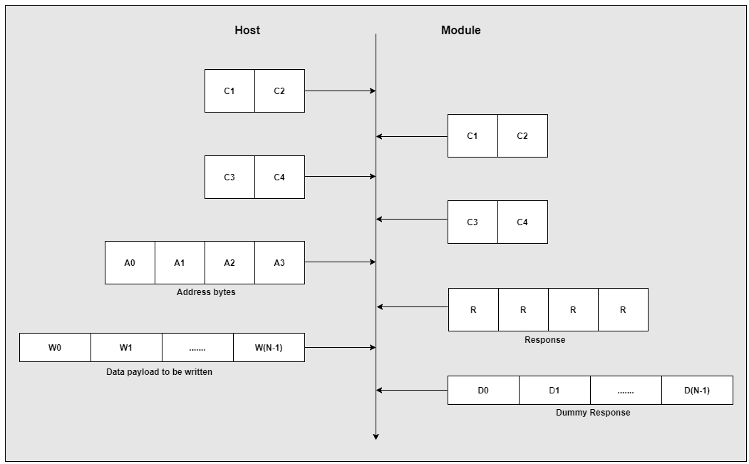
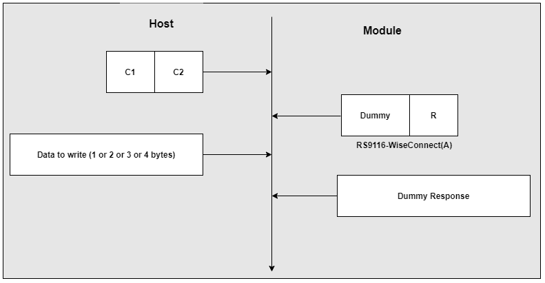
Memory Write#
The host needs access to the memory/registers of the RS9116 WiSeConnect for configuration and operation. To write data into a memory/register address, the memory write command must be framed as described in the figure below. If a "busy" or "failure" response is sent from the device, the host should either resend the command or reset the device.
Note! This structure is similar for all following read/write operations.
The host needs to follow the procedures below.
Send the commands
C1andC2.Read the response from the Device. The response appears as described in the section, SPI Response. Status
0x58indicates the device is ready.The host should send the commands
C3andC4, followed by the 4-byte address (corresponding to the memory/register address) and data. Status0x54indicates that the device is busy and the host has to retry. Status0x52indicates a failure response.
The commands C1, C2, C3, and C4 are sent in the following sequence: C1 first, then C2, C3, and finally C4. The bit ordering is as follows:
C1[7] C1[6] ... C1[0] -> C2[7] C2[6] ... C2[0] -> C3[7] C3[6] ... C3[0] -> C4[7] C4[6] ... C4[0]
C1[7] is sent first, then C1[6], and so on.
Total data payload size should be 1 byte, or 2 bytes, or multiples of 4 bytes in this operation. For example, if 5 bytes needs to be sent, it should be padded with 3 more dummy bytes to make up 8 bytes (multiple of 4) before sending.
Original data
<W0[7:0]> <W1[7:0]> <W2[7:0]> <W3[7:0]> <W4[7:0]>
Padded data
<W0[7:0]> <W1[7:0]> <W2[7:0]> <W3[7:0]> <W4[7:0]> <X5[7:0]> <X6[7:0]> <X7[7:0]>
... where X[7:0] is the dummy data.
The first byte sent is W0, the second byte sent is W1, and so on, see Bit Ordering of SPI Transactions.
Frame Write#
The sequence of command transactions (with no failure from the device) for a Frame Write is shown in the following figure. The operations are similar to memory write except that C1[3] is set and the Address phase (A0, A1, A2, A3) is skipped.
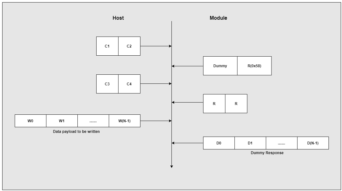
The procedure to be followed by the Host is:
Prepare and send the commands
C1,C2together as described for Frame write.Read the response from the Device.
Status
0x58indicates the Device is ready. The Host can then send the commandsC3andC4, followed by the data. Status0x54indicates the device is busy and the host must retry. Status0x52indicates a failure response.
Total data payload size should be 1 byte, or 2 bytes, or multiples of 4 bytes in this operation. For example, if 5 bytes needs to be sent, it should be padded with 3 more dummy bytes to make up 8 bytes (multiple of 4) before sending.
Original data
<W0[7:0]> <W1[7:0]> <W2[7:0]> <W3[7:0]> <W4[7:0]>
Padded data
<W0[7:0]> <W1[7:0]> <W2[7:0]> <W3[7:0]> <W4[7:0]> <X5[7:0]> <X6[7:0]> <X7[7:0]>
... where X[7:0] is the dummy data.
The first byte sent is W0, the second byte sent is W1, and so on, see Bit Ordering of SPI Transactions.
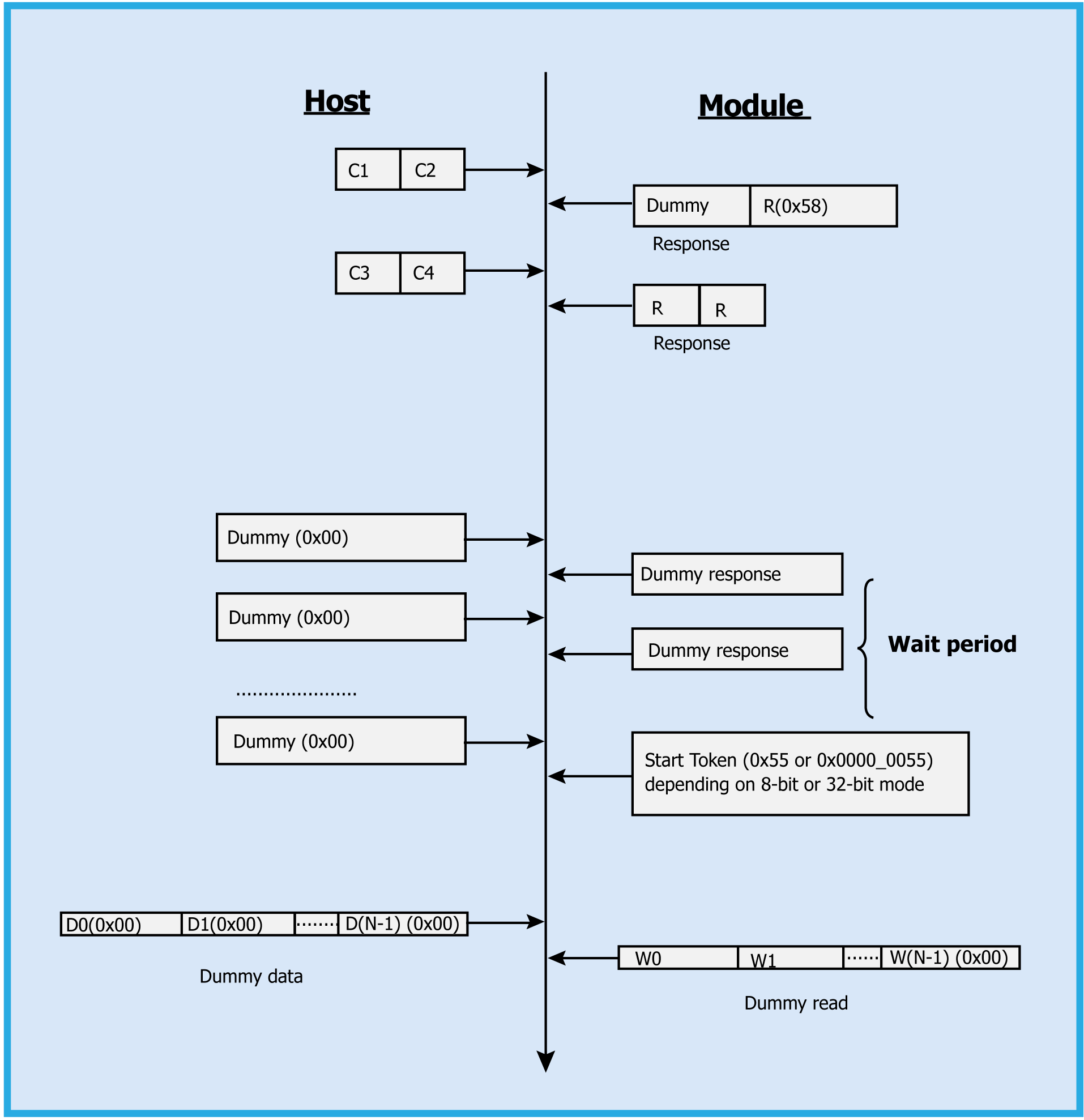
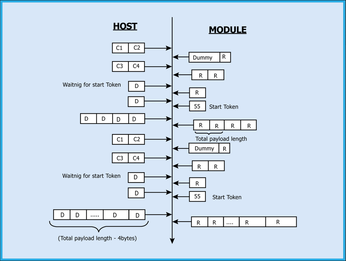
Memory Read#
To read data from a memory/register address, the host must send a Memory Read command. The following figure describes the flow for memory reads between the Host and the Device.
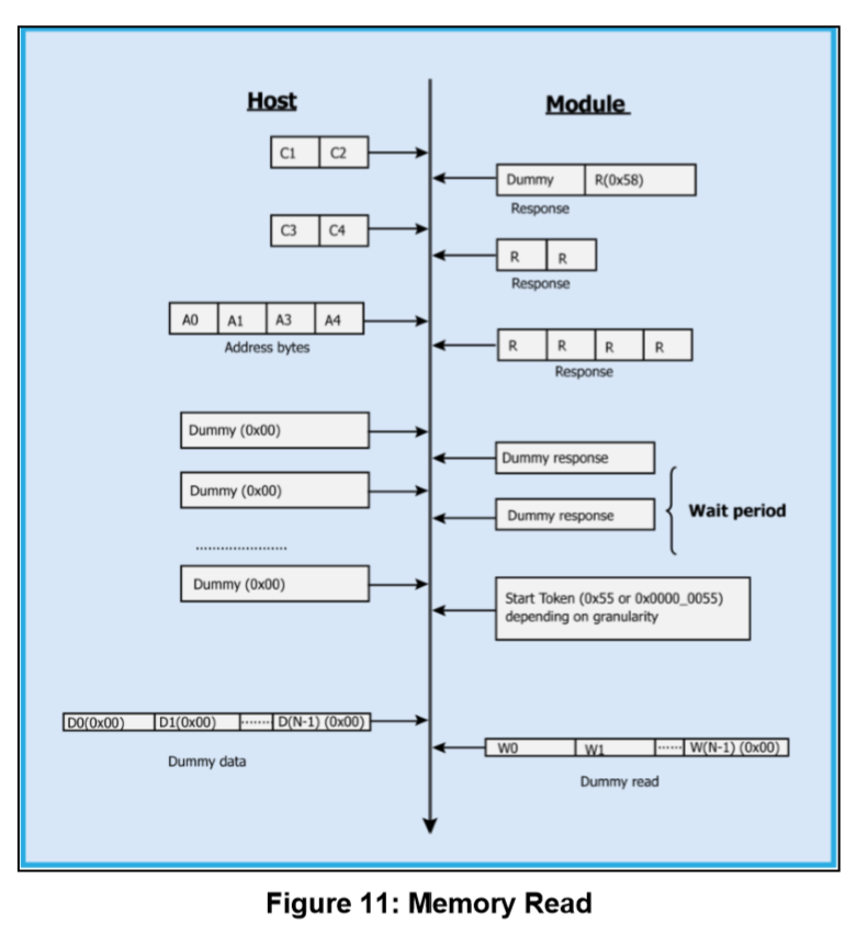
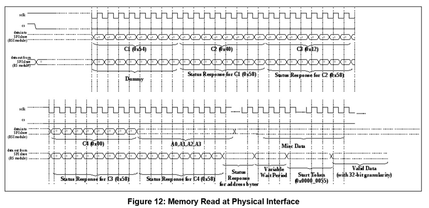
To perform a memory read, the host must follow the procedure below.
Prepare and send the commands
C1andC2.Read the response from the Device.
Status
0x58indicates the secondary is ready. The host should next send the commandsC3,C4, which indicate the length of the data to be read, followed by the address of the memory location to be read.After sending/receiving
C3,C4commands/response and the addresses, the host should wait for a start token0x55. The host writes a stream of dummy bytes to read the data from the device each time. The Host should also read this data until the start token is received. Data following the start token should be interpreted as the frame of a specified length that is read from the Device.Status
0x54, afterC1andC2bytes, indicates that the device is busy; the host should resend the read command.Status
0x52, afterC1andC2bytes, indicates a failure response from the Device.
Dummy data is sent during a variable wait period. After this period, a start token is transmitted from the Device to the Host and is followed by valid data. The start token indicates the beginning of valid data to the Host. To read out the valid data, the host must send dummy data i.e., [D0, D1, D2 ... D(N-1)]. Where N is the number of 8-bit or 32-bit dummy words (based on the mode selected), which the host needs to send to receive a specified length of valid data from the device. The commands C1, C2, C3 and C4 are sent in the following sequence: C1 first, then C2, C3, and finally C4. See, Bit Ordering of SPI Transactions for details.
The bit ordering is
C1[7] C1[6] ... C1[0] -> C2[7] C2[6] ... C2[0] -> C3[7] C3[6] ... C3[0] -> C4[7] C4[6] ... C4[0]
That is, C1[7] bit is sent first, then C1[6] and so on.
If <D3[7:0]> <D2[7:0]> <D1[7:0]> <D0[7:0]> is the data read, then D0 is sent from device first, then D1 and so on as follows:
D0[7] D0[6] ... D0[0] -> D1[7] D1[6] ... D1[0] -> D2[7] D2[6] ... D2[0] -> D3[7] D3[6] ... D3[0]
Frame Read#
Frame read is the same as Memory read, except that C1[3] is set and the Address phase is skipped. The sequence of command transactions (with no failure from the Device) for a Frame Read is described in the figure below.
To perform a Frame Read, the host must follow the procedure below.
Prepare and send the commands
C1andC2, as described for the Frame Read.Read the response from the RS9116-WiSeConnect.
Status
0x58indicates that the Device is ready. The host should send the commandsC3andC4, which indicate the length of the data to be read.After sending/receiving
C3andC4commands/response, the host should wait for a start token0x55. Data follows the start token. The host writes a dummy byte to read the data from the device each time. The Host should read this data until the start token is received. Data following the start token should be interpreted as the frame of a specified length that is read from the Device. Status0x54, afterC1andC2bytes, indicates that the device is busy and the host must retry. Status0x52, afterC1andC2bytes, indicates a failure response from the device.
The commands C1, C2, C3, and C4 are sent in the following sequence: C1 first, then C2, C3, and finally C4. See, Bit Ordering of SPI Transactions for details. The bit ordering is
C1[7] C1[6] ... C1[0] -> C2[7] C2[6] ... C2[0] -> C3[7] C3[6] ... C3[0] -> C4[7] C4[6] ... C4[0]
That is, C1[7] bit is sent first, then C1[6] and so on.
If <D3[7:0]> <D2[7:0]> <D1[7:0]> <D0[7:0]> is the data read, then D0 is sent from device first, then D1 and so on as follows:
D0[7] D0[6] ... D0[0] -> D1[7] D1[6] ... D1[0] -> D2[7] D2[6] ... D2[0] -> D3[7] D3[6] ... D3[0]
Register Read#
Register Read commands are used to read the registers in the device using the internal register address. Register read commands, such as C1 and C2 are only needed to send to the device (i.e., C3, C4, and address phases are skipped). The C2 command bits [5:0] should be the SPI internal address of the register. To read data from the registers, follow the sequence below: 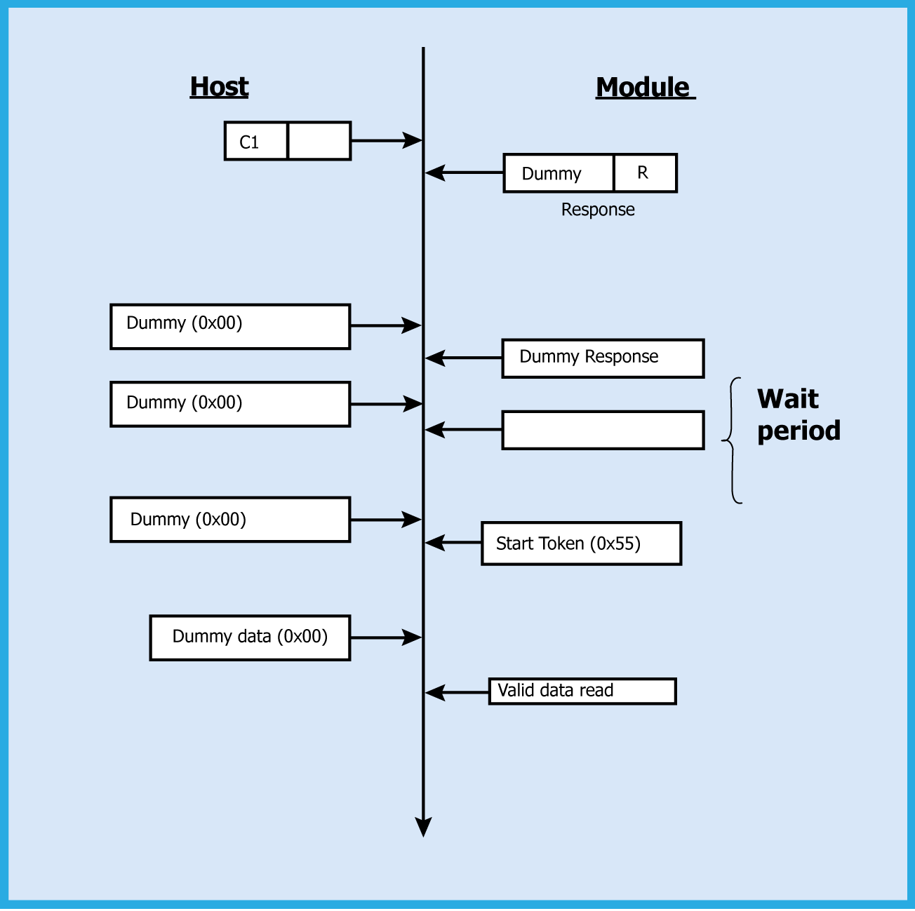
Register Writes#
Register write commands are used to write data to the registers in the device by using the internal register address. To write registers, the host needs to send C1 and C2 followed by the data to the device (i.e., C3, C4, and address phases are skipped). The C2 command bits [5:0] should be the SPI internal address of the register. To write to registers, follow the sequence shown below:
Register | Address |
|---|---|
SPI_HOST_INTR | 0x00 |
Device registers can be accessed from the host by using register read / write commands.
SPI Host Interrupt Register#
Bit | Access | Function | Default Value | Description |
|---|---|---|---|---|
[7:0] | Read only | SPI_HOST_INTR | 0x00 | These bits indicate the interrupt status value Bit 0: If '1', Buffer Full condition reached. When this bit is set, the host shouldn't send data packets . This bit has to be polled before sending each packet Bit 1: Reserved Bit 2: Reserved Bit 3: If '1', indicates data packet or response to Management frames are pending. This is a self-clearing bit, which is cleared after the packet is read by host. Bit 4: Reserved Bit 5: Reserved Bit 6: Reserved |
Software Protocol#
This section explains the procedure the host needs to follow to send Wi-Fi commands to the device and to receive responses from the device.
TX Operation#
The Host uses TX Operations to send:
management commands to the device from the Host.
data to the device, which will be transmitted onto the air.
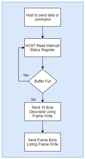
The host should follow the steps below to send the command frames to the Device:
Check the buffer full condition by reading the interrupt status register using register read.
If the buffer full bit is not set in the interrupt status register, send the Command frame in two parts:
First, send the 16-byte Frame descriptor using the Frame write.
Second, send the optional Frame body using the Frame write.
Note! Frame write is an API provided to the host as part of the SDK.
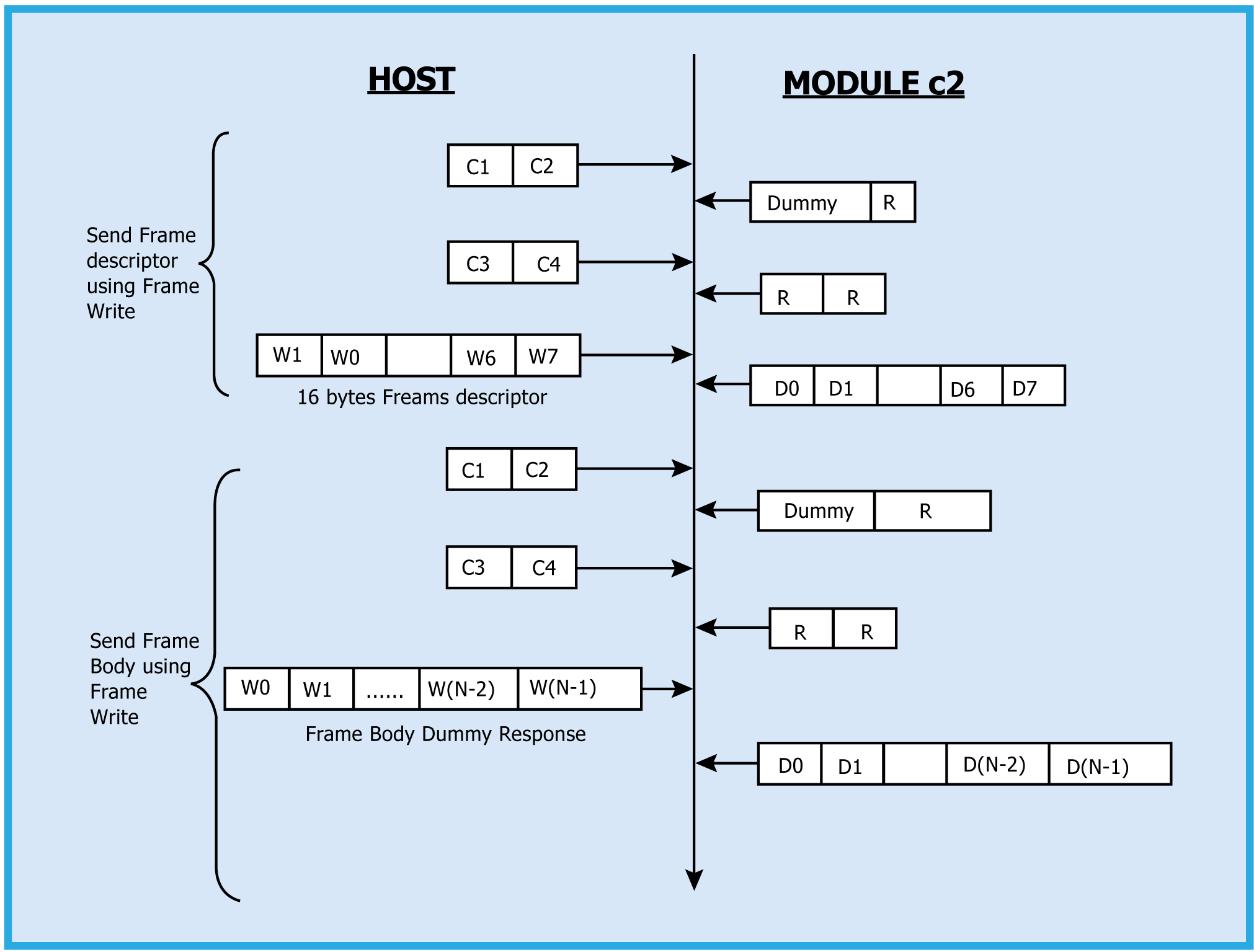
Management / Data Frame Descriptor and Frame body of command frames are sent to the device by using two separate frame writes, as shown below:
RX Operation#
The Host uses this operation:
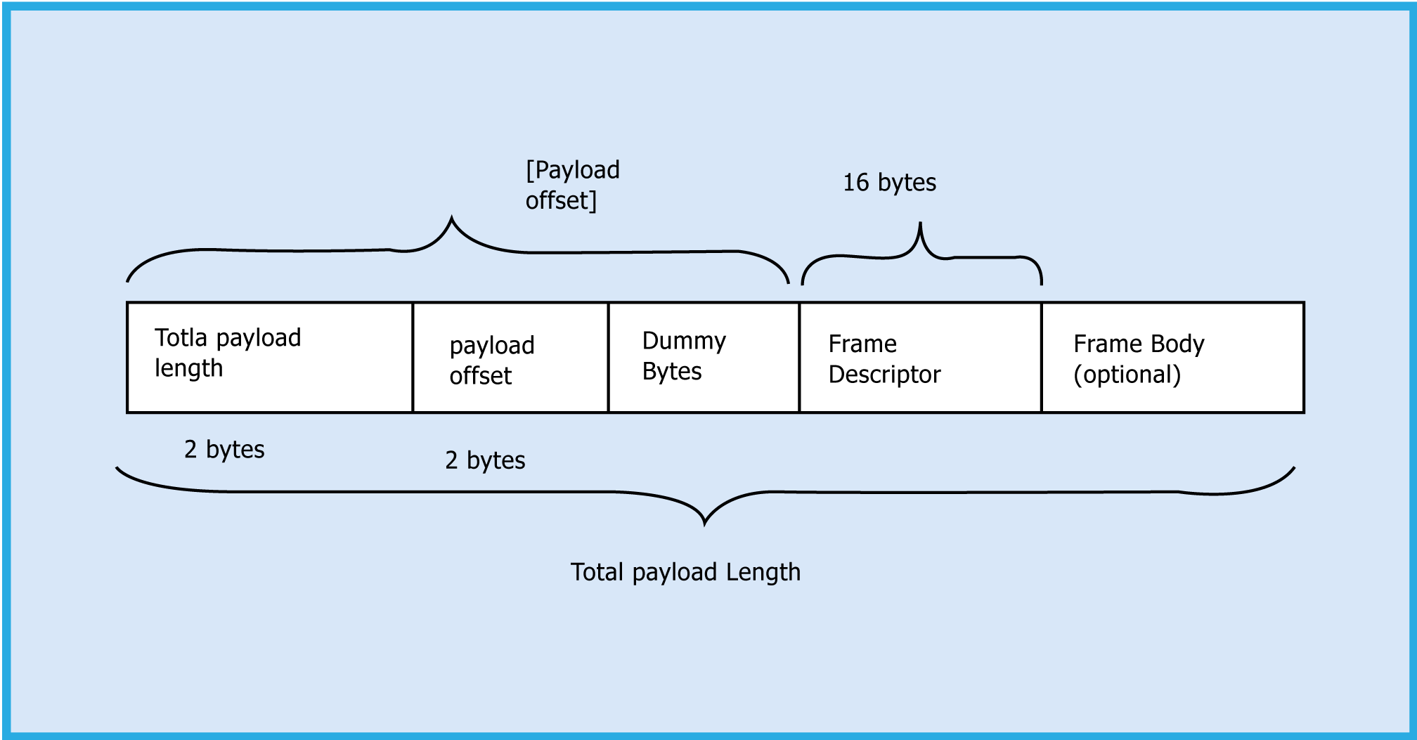
If the payload offset is x, x-4 dummy bytes are added before the Frame Descriptor.
The host should follow the steps below to read the frame from the Device:
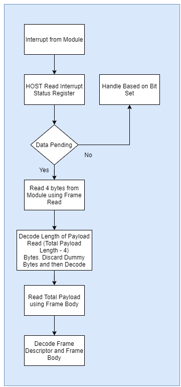
If any Data / Management packet is pending from the device, the device raises an interrupt to the Host.
The Host checks the reason for the interrupt by reading the interrupt status register using the register read.
If the data pending bit is set in the interrupt status register, follow the steps below:
Read 4 bytes using the Frame read.
Decode the total payload length and payload offset.
Read the remaining payload by sending the Frame to read with (total payload length - 4 bytes), discard Dummy bytes, and decode the Frame descriptor and Frame Body.
UART Interface#
This section describes RS9116-WiSeConnect UART interface, including the commands and processes to operate the device via UART. The UART on the Device is used as a host interface to configure the device and to send data and also to receive data.
Features
Hardware flow control (RTS/CTS)
Baud rates
9600 bps
19200 bps
38400 bps
57600 bps
115200 bps
230400 bps
460800 bps
921600 bps
Note! For baud rates greater than 115200, it is mandatory to enable UART hardware flow control.
Hardware Interface#
RS9116W uses TTL serial UART at an operating voltage of 3.3 V. Host UART device must be configured with the following settings:
Data bits - 8
Stop bits - 1
Parity - None
Flow control - None
Software Protocol#
This section explains the procedure that the host needs to follow to send commands frames to the device and to receive responses from the device.
TX Operation#
The Host uses TX operations as follows:
To send management commands to the device from the Host.
To send actual data to the device, which will be transmit onto the air.
If the host receives error code indicating packet dropped, the host must wait for a while and send the next command /data.
The host should send next data packet only if it receives ACK frame for the previous one.
The host should follow the steps below to send the command frames to the Device:
First, send the 16-byte Frame descriptor using the Frame write.
Second, send the optional Frame body using the Frame write.
RX Operation#
The device responds with a frame of the same frame type (with or without an error code in the error code field). The Host uses this operation:
Device respond, for the commands.
To read data received by device from remote peer.
Receive asynchronous information from RS9116W device.
Device send/receive data to/from Host with the following format:
If the Payload offset is x, x-4 dummy bytes are added before the Frame Descriptor.
Host should follow the steps below to read the frame from the Device: Read 4 bytes using the Frame read.
Decode the total payload length and payload offset.
Read the remaining payload by sending the Frame to read with (total payload length - 4 bytes), discard Dummy bytes and then decode the Frame descriptor and Frame Body.
SDIO Interface#
WiSeConnect SDIO interface, including commands and processes to operate the module via SDIO. RS9116-WiSeConnect supports SDIO interface which allows host to configure and send/receive data through the module via SDIO port.