Appendix: Silicon Labs Dual Polarized Antenna Array Board (BRD4191A)#
Reference Design Overview#
Geometrically, the BRD4191A is a 4x4 rectangular antenna array in shape with dimensions 160 x 160 mm. The board has 16 Dual Polarized (DP) antenna patches, each consisting of one vertical and another horizontal polarized antenna elements, resulting in a total of 32 antennas (shown in gold in the figure below).
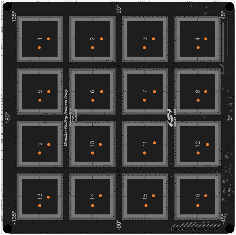
In addition to receiving signals with single orientation—either horizontal or vertical polarization, the DP antenna board also allows for the reception of Circular Polarized (CP) signals on two of the antenna patches, namely antenna 6 and 13. The CP capability is important for accurate estimation of the optimal Automatic Gain Control (AGC) value at the receiver, ensuring optimal signal strength and minimal signal distortion. For this reason, one of these antennas is switched in CP mode to receive the Bluetooth packets.
The CP is realized by driving the signals from horizontal and vertical components of either antenna 6 or antenna 13 simultaneously and combining them using a hybrid coupler while creating a 90-degree phase shift between them. For more details, refer to AN1195: Antenna Array Design Guidelines for Direction Finding.
Antenna RF Switch Structure#
The switching of the 32 antennas is done using a chain of RF switching blocks shown below.
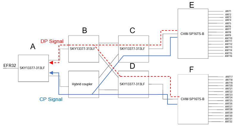
SKY switch A is used to select between CP and DP signal sources.
SKY switch B is used to select one of the CHW switches in DP mode (i.e E or F).
SKY switches C & D are used to switch two antennas simultaneously in CP mode.
CHW switches E&F are used to select one of the 16 antennas on their respective sides.
Antenna Control Pins#
In the reference design hardware, there are 7 control (CTRL) pins that can be toggled to switch antennas, select between CP and DP modes, and choose the mode of operation to AoA or AoD with ease. The functionality of the CTRL pins are:
Control pin signals CTRL1 to CTRL4 (i.e bits 0 to 3) select one of the 16 antennas on switches E & F simultaneously.
Control pin signal CTRL5 (i.e bit 4) selects either switch E or F in DP mode.
Control pin signal CTRL6 (i.e bit 5) selects either CP or DP mode (0 for DP & 1 for CP mode).
Control pin signal CTRL7 (i.e bit 6) selects either AoA or AoD mode (0 for AoA & 1 for AoD mode).
Antenna Switching#
The antenna switching is initiated by the Bluetooth stack when a BLE packet with cteInfo field present is received. A BLE packet with a CTE has the following structure.
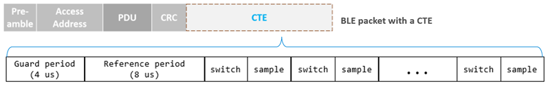
The CTE samples during the reference period are captured using one antenna, namely the reference antenna. The reference period samples are used to determine the frequency offset between the transmitter and receiver. It is important that the reference antenna is not cross polarized with the transmitter antenna. To avoid cross polarization, the reference antenna should always be selected as CP antenna. Once the phase compensation is determined, the samples in the reference period are discarded and will not be included in the angle calculation.
After the reference period, the IQ sampling is done by switching the antennas according to the switching pattern provided to the Bluetooth stack. From the estimator perspective, the RTL library expects the samples be provided so that the vertical element comes first followed by the corresponding horizontal counterpart. For example, if the switching is to be done in sequence starting from antenna ANT1 to ANT16, the samples should be fed to the algorithm in the order: {ANT_V1, ANT_H1, ANT_V2, ANT_H2, …, ANT_V16, ANT_H16}, where ANT_Vi, and ANT_Hi represent the vertical and horizontal elements of antenna patch i on the board.
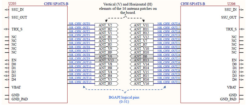
The design decisions made for optimal performance and simplicity of the antenna board, such as maintaining equal lengths of the antenna feeding lines and the CP mode of operation, came with a tradeoff in the pin mapping complexity. As a result, there is no logical sequential relation between the antenna numbering and the BGAPI pin logic sequence. Figure 4 illustrates the feed lines from the RF switches E & F to the 32 antennas (16 vertical and 16 horizontal polarized antennas) with respect to their logical pin numbers. Based on Figure 4, the switching pin pattern for the default antenna switching sequence ANT1 to ANT16 becomes:
{2, 3,0, 1,14, 15,12, 13,4, 5,8, 24,20, 21,10, 11,6, 7,22, 23,16, 17,19, 18,9, 25,26, 27,28, 29,31, 30}
In summary, the relationship between the antenna switching sequence (index starting from 0) and the logical switching pattern can be represented by the following table.

There is a helper function defined for mapping the antenna switching sequence to the switching pin control logic of this board in the RTL library: sl_rtl_aox_convert_switch_pattern(). Refer to the API reference manual to learn more about its usage.
The logical pin for the CP antenna is defined based on the bitwise operation of CTRL6 (i.e bit 5) and the logical pin of either antenna 6 or 13 —which results 40 for ANT6 and 41 for ANT13.
#define CP_MODE (1 << 5)
#define ANT6_CP (CP_MODE | 8)
#define ANT13_CP (CP_MODE | 9)