Enhanced General-Purpose Input/Output (EGPIO) Architecture#
The enhanced general-purpose input/output (EGPIO) subsystem on SiWx917 devices provides flexible digital I/O interfaces for controlling external hardware such as sensors, actuators, and communication modules.
This section describes the GPIO architecture, software layers, and power domains of the SiWx917 system-on-chip (SoC).
Peripheral Overview#
The SiWx917 SoC supports up to 45 configurable GPIOs, depending on the package type. For details on GPIO availability by package, see the SiWx917 Data Sheet.
Unused GPIO registers in smaller packages are reserved.
GPIO pads can be controlled by the following domains:
MCU high-performance (HP) domain for main application execution.
MCU ultra-low-power (ULP) domain for low-power functions and wake-up monitoring.
Network processor (NWP) for networking-related tasks when enabled.
GPIO Types#
GPIO Type | Description | Typical Use Cases |
|---|---|---|
HP GPIOs | Up to 30 pins controlled by the MCU high-performance domain. | High-speed signaling, interrupt handling, peripherals. |
ULP GPIOs | 11 pins in the low-power domain. | Sensor interfaces, low-frequency signals, wake events in PS2 and PS1. |
UULP GPIOs | 4 always-on pins powered by battery-backed supply (VBAT). | Wake-up triggers in deep sleep or retention modes. |
Enhanced GPIO (EGPIO)#
EGPIO pins support multiplexing, allowing a pin to function either as a standard GPIO or as an alternate peripheral function, such as the serial peripheral interface (SPI), universal asynchronous receiver/transmitter (UART), or pulse-width modulation (PWM).
Flexible mapping of peripheral signals
Reduced pin limitations on small packages
Software-controlled configuration through WiSeConnect drivers
Digital Signal Fundamentals#
GPIO pins operate using binary voltage levels that represent logic states:
Term | Definition |
|---|---|
HIGH | Logical 1; typically 1.8 V or 3.3 V depending on pad voltage. |
LOW | Logical 0; ground level. |
Voltage thresholds | Determine valid HIGH/LOW transitions. |
Pins support input, output, or bidirectional modes depending on your configuration.
GPIO Direction and Pad Configuration#
Each GPIO pin can be configured independently with the following characteristics:
Input mode for reading digital signals from external devices
Output mode for driving logic levels to LEDs, sensors, or integrated circuits (ICs)
Bidirectional mode for dynamically switching between input and output
Pad attributes such as drive strength, pull-up or pull-down resistors, and slew rate settings.
The WiSeConnect SDK APIs allow you to configure these parameters to meet the electrical and timing requirements of your design.
Key Features#
The SiWx917 GPIO peripheral supports:
Independent set, clear, and toggle operations for each pin
Separate mode and direction configuration per GPIO
Edge and level detection for generating interrupts
Support for 8 pins and 2 group interrupts on MCU HP EGPIOs
GPIO Software Architecture#
GPIO software uses a layered architecture that abstracts hardware details and provides a unified application programming interface (API) for SiWx917 applications.
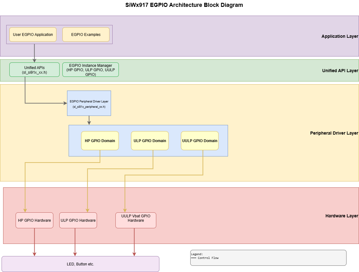
Software Layers#
Layer | Description |
|---|---|
Application Layer | User application that reads inputs, toggles outputs, and handles interrupts. |
Unified API Layer | High-level driver API ( |
Peripheral Driver Layer | Low-level access to hardware registers ( |
Hardware Layer | Physical GPIO and EGPIO blocks inside the SiWx917 SoC. |
This structure enables portable code development without needing to manipulate registers directly.
Directory Structure in WiSeConnect SDK#
The GPIO drivers in the WiSeConnect SDK follow this structure:
wiseconnect/
├── components/
│ └── device/silabs/si91x/mcu/drivers/
│ ├── unified_peripheral_drivers/
│ │ ├── inc/sl_si91x_peripheral_gpio.h
│ │ └── src/sl_si91x_peripheral_gpio.c
│ └── unified_api/
│ ├── inc/sl_si91x_driver_gpio.h
│ └── src/sl_si91x_driver_gpio.c
├── examples/
│ └── si91x_soc/peripheral/
│ ├── sl_si91x_gpio_example
│ ├── sl_si91x_gpio_group_example
│ ├── sl_si91x_gpio_ulp_example
│ ├── sl_si91x_gpio_uulp_example
│ ├── sl_si91x_ulp_gpio_example
│ └── sl_si91x_detailed_gpio_exampleClock and Power Management#
The WiSeConnect SDK and Simplicity Studio automatically manage GPIO clocking and power when GPIO components are added to a project.
Power Domain Overview#
GPIO availability depends on the system’s current power state.
Domain | Description | Active In |
|---|---|---|
MCU HP | High-performance domain for real-time tasks. | PS3 and PS4 |
MCU ULP | Low-power domain for sensing and wake logic. | Most low-power modes except deep sleep |
UULP (VBAT) | Always-on domain for lowest-power event detection. | All power states |
ULP and UULP GPIOs allow continued monitoring of external events while the system is in sleep modes.
GPIO Pin Multiplexing#
The SiWx917 features extensive pin multiplexing, allowing GPIO pins to operate either as standard digital I/O or as peripheral functions such as inter-integrated circuit (I2C), SPI, UART, PWM, and other interfaces. Understanding multiplexing is essential for efficient pin allocation in resource-constrained designs.
Pin multiplexing enables a single physical pin to support multiple functions, controlled by a GPIO Mode register. Each GPIO can be configured to operate in different modes (map to specific peripheral functions). Note that GPIO pins 0-5, 13-14, 16-24, and 35-45 in the SoC domain, ULP_GPIO_3 in the ULP domain, UULP_GPIO_4 in the UULP domain are not accessible for general-purpose application use. Only the GPIO pins explicitly listed in the pin multiplexing tables are available for configuration.
Note: For complete multiplexing tables and mode assignments, see Section 6.3 of the SiWx917 Data Sheet.
SoC GPIO Pin Multiplexing#
SoC GPIOs (GPIO_6 through GPIO_57) are available in normal operating modes (power states 4 and 3).
The digital GPIOs SOCPERH_ON_ULP_GPIO_0 through SOCPERH_ON_ULP_GPIO_11 are mapped onto physical ULP GPIOs for SoC Peripheral functionality. Similarly, ULPPERH_ON_SOC_GPIO_0 through ULPPERH_ON_SOC_GPIO_11 are mapped onto physical SoC GPIOs for ULP Peripheral functionality.
For more information about SoC GPIO pin multiplexing options, see Section 6.3.1 of the SiWx917 Data Sheet.
ULP GPIO Pin Multiplexing#
ULP GPIOs (ULP_GPIO_0 through ULP_GPIO_11) operate in the normal operating modes (power states PS4 and PS3) and also in ultra-low power mode of operation of the microcontroller (power states PS2 and PS1).
Each ULP GPIO's pin function is controlled by the GPIO Mode register in the ULP GPIO section of the Reference Manual. All ULP GPIOs can be used for analog functions when mode 7 is selected.
For more information about ULP GPIO pin multiplexing, see Section 6.3.2 of the SiWx917 Data Sheet for complete ULP GPIO pin multiplexing details.
UULP VBAT GPIO Pin Multiplexing#
UULP VBAT GPIOs (UULP_VBAT_GPIO_0 through UULP_VBAT_GPIO_3) operate in the normal mode (power states PS4 and PS3), in ultra-low power mode (power states PS2 and PS1), and also in retention and deep sleep modes.
For information about UULP VBAT GPIO pin multiplexing, see Section 6.3.3 of the SiWx917 Data Sheet
Practical Multiplexing Examples#
Understanding how peripherals map to GPIO pins helps you plan pin allocation and avoid conflicts.
Example 1: USART0 Instance Pin Usage#
The following table shows the GPIO pins utilized when the USART0 peripheral is enabled based on mode selection:
USART0 Signal | GPIO Pin (Mode 2) |
|---|---|
USART0_TX | GPIO_15 |
USART0_RX | GPIO_10 |
USART0_CLK | GPIO_8 |
USART0_CTS | GPIO_6 |
USART0_DTR | GPIO_7 |
USART0_RTS | GPIO_9 |
USART0_DCD | GPIO_12 |
USART0_DSR | GPIO_11 |
Implications:
GPIOs 6, 7, 8, 9, 10, 11, 12, and 15 become unavailable for standard GPIO operations when USART0 is active in Mode 2.
These pins cannot simultaneously serve other Mode 2 peripheral functions.
If your design requires fewer USART0 signals (for example, only TX/RX), the remaining pins can be left in GPIO mode or used for other functionality, as shown in the pin mux table.
Example 2: ADC (Analog) and GPIO Multiplexing Conflicts#
When using analog functions on GPIOs 25-30 (Mode 14), or ULP GPIOs in analog mode (Mode 7), those pins become dedicated to analog input and cannot function as digital I/O:
Pin | Analog Function (Mode) | Digital GPIO Unavailable |
|---|---|---|
GPIO_25-30 | Analog functionality (Mode 14) | Yes |
ULP_GPIO_0 - ULP_GPIO_11 | Analog functionality (Mode 7) | Yes |
Conflict Resolution Strategy:
Identify all required peripheral functions first (UART, SPI, I2C, PWM, and ADC).
Map them to available GPIO pins using the multiplexing tables.
Check for overlapping pin assignments.
Reassign peripherals to alternative GPIO pins where possible.
Multiplexing Configuration Best Practices#
Review the data sheet tables early. Before finalizing your hardware design, carefully review the tables in Section 6.3 of the SiWx917 Data Sheet to understand all available pin functions.
Plan for conflicts. Create a pin assignment spreadsheet listing all peripherals, their required pins, and alternative options to identify conflicts before implementation.
Use alternative modes. Many peripherals can operate on multiple GPIO sets. If one set conflicts with another peripheral, switch to an alternative mode.
Consider power domains. ULP and UULP GPIOs are essential for low-power operation. Reserve these for wake-up sources and low-power peripherals rather than high-speed interfaces.
Test pin conflicts early. Use the WiSeConnect GPIO examples to validate your pin configuration before integrating into your full application.
Dependencies#
Before using GPIO features, ensure:
Your Simplicity Studio project includes the GPIO component in its
.slcpconfiguration.The WiSeConnect SDK drivers are available and initialized.
The active power states support the configured GPIO type (HP, ULP, or UULP) to ensure proper operation.
For a detailed setup and initialization walkthrough, see the GPIO Initialization and Configuration Guide, which describes component setup, code generation, and pin configuration.