Development of the EFR32 Long Range PHYs#
The fundamental approach to extend usable range in the LR Profile was to decrease receiver bandwidth, while keeping key signal parameters for the demodulator, such as modulation index for FSK, intact. A few rules of thumb help to visualize what was available for this effort:
Reducing bandwidth by half improves sensitivity by 3 dB
Reducing bandwidth by 90% (to 1/10th of the original) boosts sensitivity by 10 dB
A straightforward compromise to achieve bandwidth reduction is to decrease the data rate. By cutting bandwidth in favor of sensitivity, one has to also contend with the resulting degradation in frequency offset tolerance. Moreover, such narrow-band PHYs require very accurate and stable clock references (for example, a 0.5 ppm TCXO), and those elements are more costly. In terms of RF immunity, the effect of going narrow band is mixed, with some improvement in selectivity and blocking offset by extended exposure time to interferers due to the reduced data rate.
Importantly, all of these drawbacks can be mitigated by using Direct Sequence Spectral Spreading (DSSS). This technique, which is available for all major modulation formats on the EFR32, is explored in the following section.
DSSS: Theory of Operation#
DSSS is a technique to increase the bandwidth of a transmitted signal, and thereby decrease its power spectral density. It is beneficial for the receiver side as well, as the robustness (immunity against interferer signals) significantly improves. This section reviews the DSSS implementation on EFR32 Series 1 devices.
TX Side#
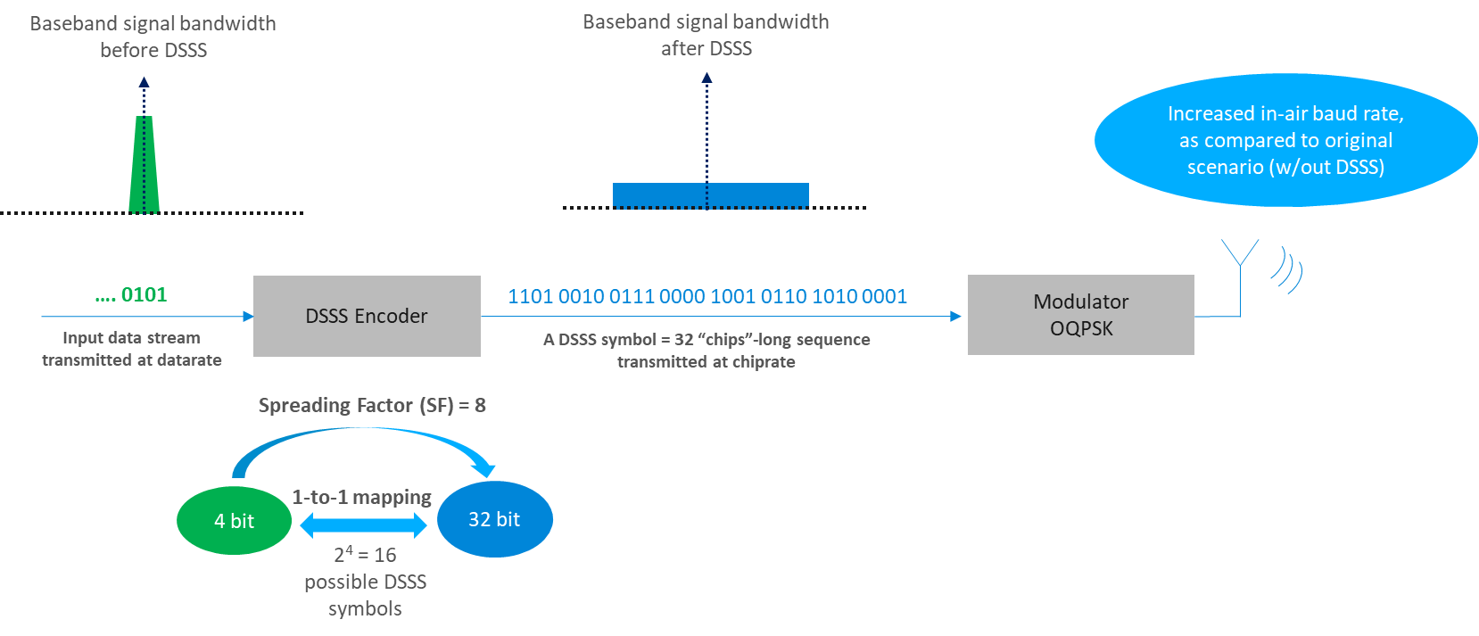
The above figure shows how a DSSS-based signal is constructed. As a practical demonstration vehicle, this example uses the 802.15.4 Zigbee packet format.
The baseband input signal is a narrow band, low data rate signal stream (its spectrum plot represented by the green cone). This bitstream is fed into a DSSS encoder, which replaces every 4 bits of the bitstream with a 32-bit symbol, often referred to as 32 “chips”.
Transmitting 1 symbol takes the same amount of time as transmitting 4 bits of the original data stream. This means that the “chip rate” is 8x higher than the original data rate, a multiplier often referred to as the Spreading Factor.
The blue rectangle (spectrum plot of baseband input signal after DSSS encoding) demonstrates that the original narrow band signal has become much wider (though not quite 8x), with less power density. The resulting data stream with the chip rate is then fed into the modulator and radiated over the air. Therefore, by increasing the link's in-air baud rate, the same data can be transmitted with the same net data rate, over the same period of time, but using a much wider band and lower power spectral density.
RX Side#
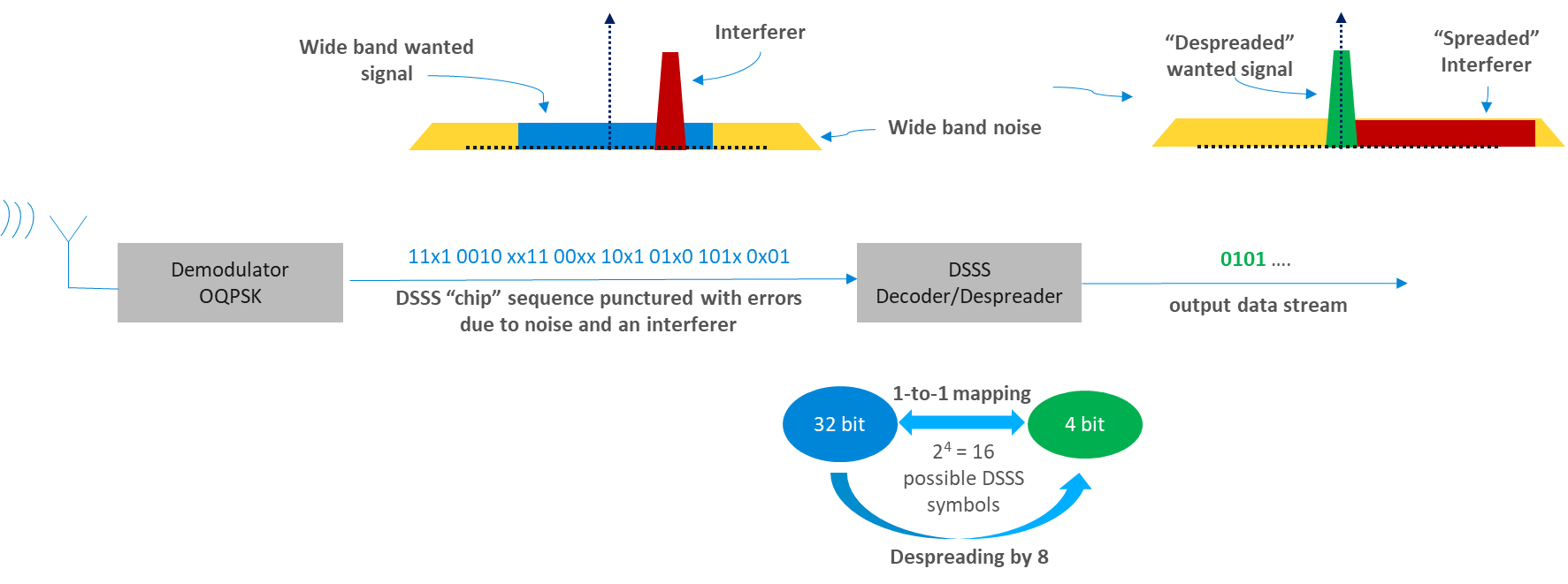
The above figure shows reception of the DSSS-encoded transmission detailed in the previous section. The demodulator retrieves the data stream from the OQPSK signal. The bits are changing with the chip rate, and the stream may contain errors due to the presence of noise and interferers in the air.
The plot at the top left corner of the above figure demonstrates the spectral conditions while receiving a DSSS packet. The red pyramid indicates the presence of a strong narrowband interferer, while the yellow trapezium represents the wideband noise.
This corrupted chip stream is fed into the DSSS Decoder, which replaces every 32-chip long symbol with a 4 bit pattern, thus restoring the original data stream. Despite errors in the chip stream, the decoder can still identify the correct 32-chip symbols due to the 8x redundancy presented by the scaling factor.
The spectrum plot at the top right corner of the figure shows that the original green cone has been restored by this de-spreading procedure, while the red cone has been “smeared” with the noise. As a result, SNR is increased, which compensates for the increased noise power experienced by the demodulator due to the high in-air bandwidth.
DSSS: Practical Impacts#
As a result of using DSSS, an application is subject to the following considerations:
Co-channel and adjacent channel selectivity improve by a factor of the coding gain (3 to 8 dB, depending on spreading factor)
A less accurate (cheaper) crystal can be used for the clock reference
Higher TX power can be used in cases where the regulatory limit is defined as maximum allowed power spectral density
DSSS alone does not technically improve RX sensitivity to in-air signals:
Receiving a 1 kbps data stream exhibits the same RX sensitivity whether or not the signal content is DSSS-encoded
DSSS increases the symbol rate and bandwidth of the signal physically present in the air, which actually degrades reception at the RX side, but this consequence is compensated by the DSSS processing gain in the receiver
Scaling the 802.15.4 PHY#
To leverage the benefits of DSSS and develop robust Long Range options for EFR32 Series 1 devices, Silicon Labs began with the highly optimized 802.15.4 Zigbee PHY, and derived a series of radio configurations to serve a variety of sensitivity and tolerance requirements. Essentially, the data rate (and therefore the occupied bandwidth) has been scaled down, while retaining the same Zigbee coding scheme: OQPSK, DSSS SF=8, and 32-bit symbol length with a 4-bit symbol map. The resulting PHY configurations are available for xG12 / xG13 / xG14 variants of the Series 1 family.
The following table shows one group of PHYs optimized for a lower frequency band, and another group optimized at a higher frequency band. Notably, the stated performance is maintained when setting the carrier frequency to anywhere within each band.
The table indicates the required XO accuracy for the TX and RX side COMBINED. Practically speaking, the value in the table should be SPLIT between TX and RX sides. This presents a cost savings opportunity on nodes manufactured in large quantities vs low volume base stations, where you can asymmetrically distribute the XO accuracy budget to reduce the cost of high volume elements.
Note: The last item, 80 kbps for 915MHz, can be used to pass FCC 15.247 requirements without the need for frequency hopping, as the occupied bandwidth of the signal is > 500 kHz.
Table: PHY Configuration Options on the Long Range Profile
Frequency Band[MHz] | Data Rate[kbps] | (TX + RX) XO Accuracy[ppm +/-] |
|---|---|---|
434/490 | 1.2 | 2.5 |
434/490 | 2.4 | 5 |
434/490 | 4.8 | 10 |
434/490 | 9.6 | 20 |
434/490 | 19.2 | 40 |
868/915 | 1.2 | 1.25 |
868/915 | 4.8 | 5 |
868/915 | 9.6 | 10 |
868/915 | 19.2 | 20 |
868/915 | 38.4 | 40 |
868/915 | 80 | 40 |
Radio Boards Supporting Long Range PHY Evaluation#
Many configurations within the Long Range Profile can be successfully demonstrated on any radio board with a supported EFR32 Series 1 SoC and suitable sub-GHz band support. However, for those users who would like to test the best possible narrow band PHY configurations, radio boards that satisfy the XO requirements in the table above are also available for purchase. The following table specifies the configurations Silicon Labs currently offers.
Table: Radio Boards with TCXO
Ordering Part Number | Board ID | Board Configuration |
|---|---|---|
SLWRB4261A | BRD4261A | EFR32FG14 Dual-Band 2400 / 490 MHz +19.5dBm |
SLWRB4262A | BRD4262A | EFR32FG14 Dual-Band 2400 / 915 MHz +19.5dBm |
SLWRB4262B | BRD4262B | EFR32FG14 Dual-Band 2400 / 868 MHz +19.5dBm |
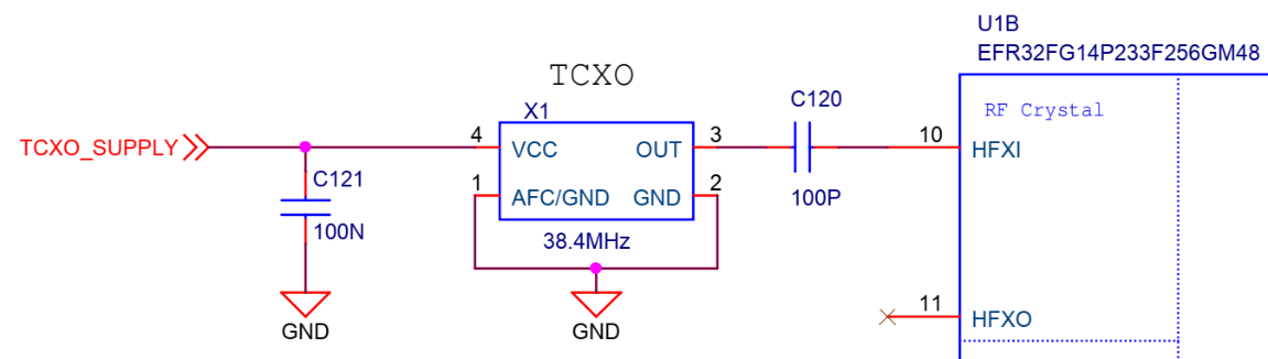
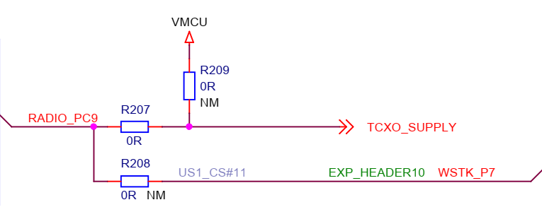
These boards are equipped with a high performance (+/- 0.5 ppm accuracy) TCXO for the HFXO reference, as shown by the schematics in the following figure. The TCXO supply is connected to pin PC9 on the SoC, which enables the EFR32 to shut down the TCXO when not in use to save power. If the customer application needs PC9 for a different purpose, the TCXO power supply can instead be connected directly to the VMCU rail (via the R209 solder dot seen in the following figure).