Programming and Debugging Interface#
EFR32ZG23 | ZGM230S |
|---|---|
Applicable | Applicable |
A programming interface is mandatory if in-system programming of a Z-Wave 800 device is required, i.e., programming a new/erased chip while soldered onto the product PCB. To design in a footprint for the Mini Simplicity header, Silicon Labs recommends using a small 10-pin, 1.27 mm SMD header for both programming and debugging chips from the Silicon Labs Gecko family.
If a connector is used, the Samtec FTSH-105-01-F-DH surface mounted or Harwin M50-3500542 through-hole male connector is recommended and can be used directly with the BRD8010A STK/WSTK Debug Adapter. The functionality of the pins from the programmer’s perspective is shown in the table below. Refer to [2] and [6] for programming instructions and more about the Mini Simplicity Header.
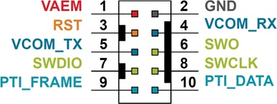
Pin Location | Pin Name | Type | Function |
|---|---|---|---|
1 | VAEM | S | Supply voltage for the circuit / Z-Wave device. If connected to a WSTK, this pin is equivalent to VAEM. |
2 | GND | S | Common ground between the programmer and Z-Wave 800 device |
3 | RST | O | Driven low by the programmer to place the Z-Wave 800 device in a reset state |
4 | VCOM_RX | O | Transmit UART serial data to Z-Wave 800 device |
5 | VCOM_TX | I | Receive UART serial data from Z-Wave 800 device |
6 | SWO | I | Serial Wire Output |
7 | SWDIO | I/O | Serial Wire Data |
8 | SWCLK | O | Serial Wire Clock |
9 | PTI_FRAME | I | Packet Trace Frame Signal |
10 | PTI_DATA | I | Packet Trace Data Signal |
Programming Interface Overview#
The table below shows which interfaces can be used to program the flash memory of the various Z-Wave 800 products:
EFR32ZG23 | ZGM230S | |
|---|---|---|
SWD programming | X | X |
Bootloader UART programming | X | X |
Notes:
Bootloader is not programmed into the chip at delivery.
SWD interface will be needed for new chips and after full chip/flash erase.