PCB Implementation#
EFR32ZG23 | ZGM230S |
|---|---|
Applicable | Applicable except IC Grounding |
A good PCB implementation is required to obtain the best performance from a Z-Wave 800 device. The following subsections describe items that should be considered when designing the PCB layout.
Besides the descriptions below, use the reference designs for the ZGM230S and the EFR32ZG23 devices as guidelines. The reference design for the ZGM230S is BRD4205B. The reference designs for the EFR32ZG23 are BRD4204D and BRD4210A.
Further layout guidelines can be found in [12].
Placement#
In general, it is mandatory that all decoupling and matching components are placed as close as possible to the Z-Wave 800 device, and on the same layer to reduce trace parasitics. For gateway devices with GSM or LTE transceivers, Silicon Labs also strongly recommends placing the SAW filter as close as possible to the EFR32ZG23 matching network or to the ZGM230S RF pin.
When implementing a Z-Wave system into a product, it is strongly recommended that the Z-Wave 800 device is placed close to a corner of the product’s PCB, away from any high frequency switching circuits used elsewhere in the product, e.g. host CPU systems, switching dc supplies, motor-controllers, etc.
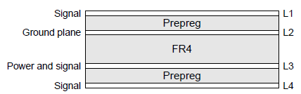
Stack-up#
If designing a product with the EFR32ZG23, Silicon Labs recommends using a 4-layer stack-up PCB as shown in the figure below. Choose the thickness of the PCB stack-up that best optimizes cost. The distance between L1 and L2 layers should be as close to 300 μm as possible. Silicon Labs strongly recommends using a solid copper plane as the ground plane layer L2.
With the ZGM230S, the complex circuitry is contained inside the SiP. Therefore, there are good possibilities for making a cheap, two-layer PCB design with ZGM230S. This does require extra care in designing the RF routing, power supply, and ground layout as no full-layer power and ground planes can be included.
Refer to the BRD4204D, BRD4205B, and BRD4210A designs for more information.
Power Routing#
Use as short VDD traces as possible. The VDD trace can be a hidden, unwanted radiator so it is important to simplify the VDD routing as much as possible and use large, continuous GND pours with many stitching vias. To achieve the simplified VDD routing, try to avoid star topology of VDD traces (i.e., avoid connecting all VDD traces in one common point).
Consider using the reference designs BRD4204D, BRD4205B, and BRD4210A as the reference designs when creating the power routing.
Decoupling#
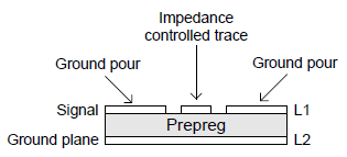
Power should be driven through decoupling capacitors to prevent parasitic inductances as shown below.
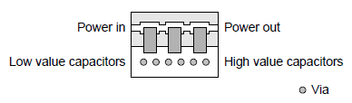
At least two grounding vias is recommended for each component as shown below.
ZGM230S SiP Module#
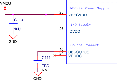
For the ZGM230S, most of the decoupling is built in. This includes all supply decoupling except for one 10 µF capacitor on VREGVDD and IOVDD combined. If high switching activity is expected on the GPIO interface, Silicon Labs recommends 10 μF on each of the supply lines (VREGVDD, IOVDD).
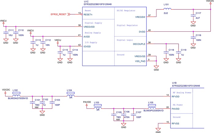
EFR32ZG23 SoC#
For an EFR32ZG23 device, Silicon Labs strongly recommends the decoupling topology shown in the figure below.
RF Trace#
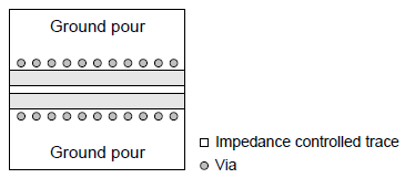
For RF traces longer than λ/16 at the fundamental frequency, it is mandatory to design the trace as a transmission line with a 50 ohm characteristic impedance. A coplanar waveguide similar to the figure below is recommended for a transmission line on signal layer L1.
A via fence is recommended on both sides of a coplanar waveguide, as shown in the following figure, to short any return currents induced on the top layer to ground.
A free tool, such as Saturn PCB Design Toolkit (http://www.saturnpcb.com/pcb_toolkit.htm), can be used to calculate the dimensions of the traces conveniently.
IC Grounding#
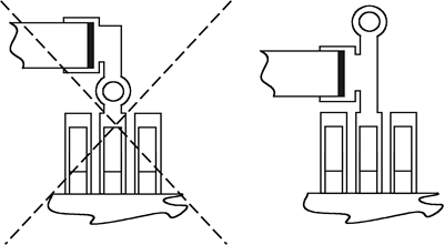
QFN chips should be provided with a ground paddle with stitched-vias to minimize parasitic inductance and to provide a good thermal heat sink as shown in the following figure.
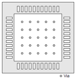
Refer to the BRD4204D or BRD4210A layout to see a practical implementation of a QFN footprint with exposed pad.