Bringing Up Z-Wave Hardware in General#
When bringing up and validating a Z-Wave 700 or 800 hardware platform, Silicon Labs provides a special software tool called RAILTest. RAILTest is part of the Z-Wave software offering, and the following versions are available:
700 series:
A version for the ZGM130S SiP module
A version for the EFR32ZG14 SoC
800 Series:
A version for ZGM230S SiP module
A version for EFR32ZG23 SoC
RAILTest eliminates the need for creating a special “Hardware bring-up” Z-Wave application, because RAILTest offers all the functionality needed to exercise the RF parts of the Z-Wave product under development.
Using RAILTest, parameters such as:
RF output power
RF frequency
Crystal fine tuning
Z-Wave sensitivity
can easily be measured on the Z-Wave hardware which is being brought up / validated. Settings for output power, etc., can be fine-tuned and afterwards incorporated in the final Z-Wave application code, thus ensuring that the performance of the Z-Wave product will live up to all customer and RF regulatory demands.
Hardware Design Consideration for Easy Bring-Up and Validation#
As a part of the general hardware design procedure for a Z-Wave product, one should take the following items into consideration:
How can the RF performance of the product be tested?
How to interface the product during the bring-up phase of the project?
How to provide means for the RF regulatory authorities to approve the product?
How to fine-tune RF parameters to obtain the best possible performance of the product?
If a solution for each of the above-mentioned items is implemented in the product at design-time, the effort of bringing up the product will be significantly reduced.
How to Test the RF Performance of the Z-Wave Product#
All Z-Wave products contain an RF antenna, and many products incorporate the RF antenna as an integrated PCB antenna.
If the product has a PCB antenna, it is not easy to measure the output power of a Z-Wave device. Such a measurement usually requires access to an anechoic chamber. However, even though it might be difficult to measure the output, this must be done to pass regulatory RF tests and to ensure that the settings of the output power matches the needs for the specific product.
At design time, the decision to add an RF connection point for such a conducted measurement can be taken.
An RF connection point can be a non-populated footprint for an RF connector, which can be switched into the RF path for conducted measurements, or it can be a PCB landing pattern for a soldered attachment of an RF coax pig-tail. If the antenna structure requires an RF matching structure, the placement of the RF matching components can serve as an RF connection point as well. See the examples below:
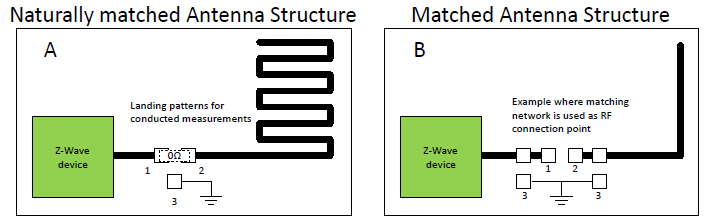
The figure above shows two examples: a product with a naturally matched antenna, A, and a product requiring a match, B. The three landing patterns shown on Product A can be used to:
Measure the output power of the Z-Wave device
Measure the RF properties of the antenna structure of the device
For normal usage, the landing patterns marked "1" and "2" on Figure 1 A are shorted by a 0 ohms resistor. Landing pattern "3" is connected to the RF ground plane of the PCB.
For product A: During bring-up of the product or when the RF regulatory authorities are to measure conducted RF power, the 0 ohms resistor is removed, and an RF pig-tail can be soldered to the landing patterns "1" and "3". The inner-core of the RF pig-tail must be connected to landing pattern "1" and the grounding shield of the RF pig-tail must be connected to landing pattern "3". The RF pig-tail can now be connected to an RF spectrum analyzer, and the output power transmitted by the Z-Wave device can be measured with a minimal insertion loss and without the need for any radiated RF power measurements.
When the RF properties of the antenna structure are to be measured, this also can be done with the usage of the landing patterns and an RF pig-tail. In this case, the 0 ohms resistor connecting landing pattern "1" and "2" must be removed, and the inner-core of the RF pig-tail must be connected to landing pattern "2" and the grounding shield of the RF pig-tail must be connected to the landing pattern "3".
Note: When measuring the parameters of the antenna structure using a network analyzer, please be aware of the effect of the cable used to conduct the measurement.
For product A, the cost for this landing-pattern connection method will be the PCB real-estate for the three landing patterns and the BOM cost of a 0 ohms resistor.
If the antenna requires an RF matching structure, such as a T or Pi configuration, see product B in the figure above. Here, the landing patterns for the matching components may serve as connections points as well. In this case, the landing pattern "1" can be used to measure the direct output power from the Z-Wave device, whereas landing pattern "2" can be used to measure the RF characteristics of the antenna structure. Again, landing patterns 3 are RF ground connections.
The benefit of this hardware design strategy, where the possibility for an RF connection point is contained in the final product design is:
Shorter bring-up time
Effortless connection of the RF pig-tail without destroying or cutting in the product
More reliable and predictable measurements
With a firmly attached RF pig-tail, measurements can be repeated and are not depending on reflections or environmental changes as with radiated measurements
Be aware of the cable effect for antenna measurements
Better possibilities to adjust the Z-Wave device for best possible performance, which creates a better product.
With a well-tuned RF product, most of the RF energy transmitted by the Z-Wave device will be radiated by the antenna-structure; therefore, the customers will experience the best possible RF range between Z-Wave products.
Note: If a non-populated RF connector is used instead of the landing pattern strategy, an even more robust and easy-to-use RF connection point can be created during the bring-up and validation phase. Then an RF connector is soldered onto the product when needed, and once finished with the prototypes, the RF connector is removed from the BOM.
How to Interface the Z-Wave Product During the Bring-Up Phase of the Project#
Since Silicon Labs strongly recommends using the software RAILTest during the bring-up and validation phase of a Z-Wave product, interfacing to the Z-Wave device is as important as being able to perform RF measurements on the product.
RAILTest is a stand-alone software package, available as a binary, and is not a part of any Z-Wave application. To use RAILTest, one must be able to flash the Z-Wave device with the software during the development phase.
If the product does not contain a host processor, a programming interface to the Z-Wave device will be an integral part of the product, and it will not be a problem to flash RAILTest to the Z-Wave device using the main programming interface of the product:
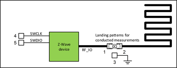
The programming pins of Z-Wave 700 devices are located at the ports PF0 and PF1, while the programming pins for Z-Wave 800 devices are located at the ports PA01 and PA02. The interface for these ports, along with supply and ground connections, etc., can be realized as a PCB connector, test points on the PCB, or landings patterns on the PCB. The method is selected depending on the requirements of the BOM cost and on how to assemble and program the Z-Wave product during the manufacturing flow. The main point is that there must be a physical programming interface available in the product.
If the product does contain a host processor, there are two possibilities for programming the Z-Wave device:
The host processor can download code to the Z-Wave device.
The host processor cannot download code to the Z-Wave device.
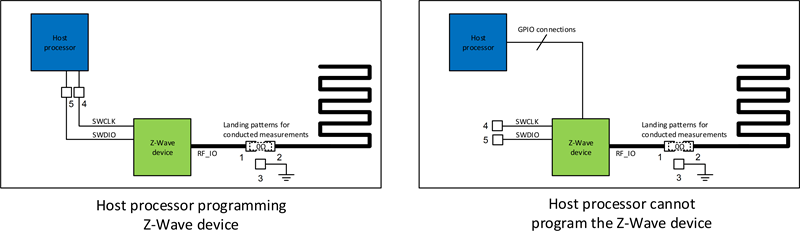
For situation #1, where the host processor can program the Z-Wave device, one must ensure that the host processor is also able to handle and download the RAILTest during the bring-up and validation phase. If this is not the case, implementing a direct programming interface to the Z-Wave device, e.g., at a set of landing patterns, is strongly advised.
For situation #2, where the host processor is not able to program the Z-Wave device, programming the Z-Wave device must be handled as if the product did not contain any host-processor at all. In this case, a connector, landing patterns, or test points must be designed in to the product for programming purposes.
Apart from the ability to download RAILTest software to the Z-Wave device, one must also be able to use and control the Command Line Interface (CLI) of RAILTest, and this requires access to the UART pins of the Z-Wave device.
For products without a host processor, the interface to the UART pins of the Z-Wave device can be a connector, a set of landing patterns, or a set of test points on the product. See the example below.
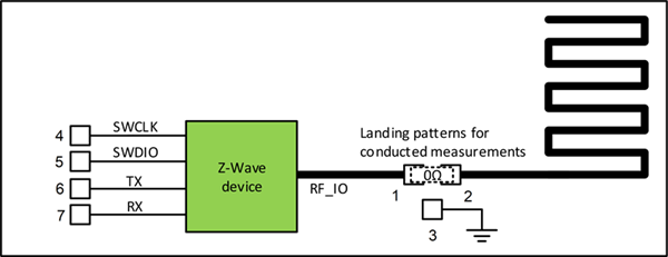
During the bring-up and validation phase, wires can be temporarily connected to the UART interface and RAILTest can be configured and controlled. The UART pins of Z-Wave 700 devices are located at the ports PA00 (UART_TX) and PA01 (UART_RX), while the UART pins for Z-Wave 800 devices are located at the ports PA08 (UART_TX) and PA09 (UART_RX).
For products with a host processor, two possibilities exist for controlling the RAILTest software through the UART interface of the Z-Wave device:
The host processor provides a terminal interface.
The Z-Wave device can be controlled directly through its UART interface.
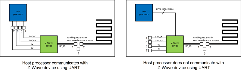
For situation #1, where the host processor uses the UART lines to control the Z-Wave device, the host processor should be able to directly relay any commands to and from the Z-Wave device. This will enable the developer to control the RAILTest software using the connection through the host processor. If this is not possible, a connection in the form of a connector, a set of landing patterns or test points, like those shown in the figure above, should be available on the product. During bring-up and validation, temporary connections to the UART connection points can make this be used to control the RAILTest software.
For situation #2, where there are no UART connections between the host processor and the Z-Wave device, it is strongly advised to provide connection possibilities to the two UART connections of the Z-Wave device, e.g., the landing patterns 6 and 7 shown in the figure above.
The cost of implementing a programming- and control-interface will depend on the method selected. If a connector is selected, and the connector is going to be permanently mounted in the product for no other reason than ensuring the interface needed for the bring-up phase, the BOM cost will be high. But, if the connector is not mounted in the finished product, or if the interface connections are realized as landing patterns or test points, the cost will only be the added real-estate of the PCB. If the programming interface and control interface are implemented as part of a host processor system, there will be no cost added at all.
The benefit of this hardware design strategy, where the needed interface connections are contained in the final product design is:
Shorter bring-up time
Effortless reprogramming and control of the product without cuts and straps
More reliable and predictable measurements
With a firmly attached programming and control interface, changes to settings can be repeated and are not dependent on dangling wires which easily break.
Better possibility for third-parties to interact with the product
Regulatory authorities can more easily handle the products during the required RF regulatory measurements since the product is not fragile.
As an example of products with added interface structures for use during both bring-up, validation and production, refer to the radio boards from the Z-Wave development kits:
700 series: BRD4206A, BRD4207A
800 series: BRD4204D, BRD4210A, BRD4205B
How to Provide Means for the RF Regulatory Authorities to Approve a Z-Wave Product
Any product containing a radio transmitting and receiving device must be approved by the appropriate RF regulatory authorities, and this is also valid for products based on the Z-Wave 700 and 800 devices.
The following RF properties are measured during an RF regulatory measurement session:
Conducted RF measurements
Performed on a CW for each Z-Wave frequency applicable for the product.
Radiated RF measurements
Performed on a CW for each Z-Wave frequency applicable for the product.
Performance measurements, such as blocking performance measurements
Performed on a simple Z-Wave system.
To obtain as efficient a measurement session at the RF regulatory authorities as possible, it is strongly advised to be well prepared:
Prepare a test product fitted with RF pig-tail/wired RF connection, RAILTest downloaded to the product, and UART interface
This product will be for the Conducted and Radiated CW measurements
Prepare a test product with the Z-Wave application downloaded to the product
This product will be for the performance measurements
Prepare a controller / companion product for the product, which can enable the product for normal Z-Wave operation
This product will be for the performance measurements
The set of pre-configured modules, the controller, and how to use and setup the device for the various tests should be described in a Standard Operating Procedure (SOP), which should be sent with the modules when they are shipped to the RF regulatory authorities.
The controller to use can be a Silicon Labs Z-Wave PC controller or it can be the controller intended for controlling the product. The most important factor is that the controller and how it is to be used in relationship to the RF regulatory measurements is described in such a way that a third party, i.e., the test personnel at the RF regulatory test lab, will be able to setup the needed test sequence.
How to Adjust RF Parameters to Get the Best Possible Performance of the Product#
Regarding adjustments and what to adjust to obtain the best possible RF performance of the product, most settings are taken care of by the Z-Wave protocol. There are, however, three settings which cannot be pre-set by the Z-Wave protocol because the settings are dependent of the layout for the product. These settings are as follows:
PA setting
The output level for the PA
Crystal calibration
Fine-tuning of the RF and system frequency
Listen Before Talk (LBT) RSSI threshold
The RF noise level threshold above which Z-Wave transmission is not allowed. Only valid for certain Z-Wave regions.
Regarding the PA setting: For each Z-Wave region, the level of RF power allowed to emit is regulated by the regional RF regulatory authorities. Both RAILTest and the Z-Wave protocol allows for setting up the PA to be able to transmit as much RF power as allowed and fulfill the requirements for the RF fundamental as well as the RF harmonics.
Setting up the transmitted RF output power level can be adjusted in RAILTest, and once the correct level is found, the setting must be transferred to the settings used in the Z-Wave protocol.
Instructions for using RAILTest for setting the PA output power are described in Using RAILtest.
Regarding the crystal calibration: Calibration/Fine adjustment of the crystal is applicable to products based on the EFR32ZG14 and EFR32ZG23 devices. For products based on ZGM130S and ZGM230S modules, no fine adjustment is needed since these modules are calibrated at production time.
What is the purpose of a system frequency calibration / fine adjustment? The tolerances of all crystals are divided into three components: (1) an initial tolerance, (2) a temperature tolerance, and (3) an aging tolerance. The initial tolerance is what can be removed by a calibration / fine adjustment of the product.
The general need for precise system frequency in a radio system arises from the fact that all receiver systems have filters in the receive path. To eliminate unwanted noise in the receiver path, the bandwidth of these receiver filters must be as narrow as possible. Therefore, a designer must make sure that the frequency variation of the transmitted signal matches the bandwidth of the receiver filters because if the transmitter varies too much, the receiver filters start to attenuate the information carrying signal. So, if both the transmitter and the receiver are aligned on the same RF frequency / system frequency, an optimal receive chain can be realized where only the information from the transmitters signal passes through the receiver filters.
There are two methods which can be used to conduct a crystal fine-tuning / calibration:
Each module is individually frequency calibrated during the manufacturing of the product
The product is generally frequency adjusted
Approach #1 results in the best possible performance of the product because it will ensure that the individual crystals are adjusted to their nominal frequencies. The drawback is a costly process to perform an inline crystal calibration during the manufacturing of a product. Note that all ZGM130S and ZGM230S devices are individually frequency calibrated during the device manufacturing process at Silicon Labs.
Approach #2 is a general frequency adjustment, which is highly recommended for the product when it is in the prototype phase. The general frequency adjustment counteracts for the parasitic load of the crystal component which varies from product layout to product layout. See the two examples below:
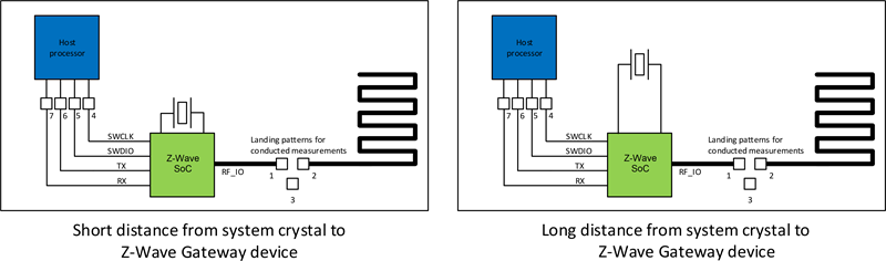
The product with the short distance between the system crystal and the Z-Wave SoC device has a relative small parasitic load capacitance compared to the product with the longer distance between the crystal and the Z-Wave SoC device.
Note: It is always recommended to keep the distance from the system crystal to the Z-Wave device as short as possible.
An internal load-capacitance can be adjusted through RAILTest or through a Z-Wave API in the Z-Wave protocol. Due to lot-to-lot variations between Z-Wave devices, a general adjustment is not possible. Each product item must be individually calibrated during the production of the product.
Refer to Using RAILtest to read more about how to perform the crystal adjustment. Read more about crystal calibration in [3].
Regarding Listen Before Talk RSSI threshold: For certain Z-Wave regions, RF regulatory authorities require that a transmitting device performs a clear channel assessment before the device can transmit any RF energy. In Japan, the LBT limit is -80dBm, and, in Korea, the limit is -65dBm. This means that Z-Wave devices must be able to measure the amount of RF energy in the channel and, if the measured RF noise level is below -80dBm, the Z-Wave device may transmit a Z-Wave frame. The same applies for Z-Wave devices in Korea, only with the limit of RF noise at -65dBm.
To compensate for any RF loss in the RF path of a Z-Wave device, the LBT thresholds -80dBm or -65dBm cannot be used directly as threshold values in the Z-Wave protocol, since this would give a too pessimistic LBT threshold. For example, if the antenna gain of the product is -2dBi and the RF path-loss after the antenna is 2.5dB, due to some matching components, the total loss in the RF path is
4.5dB. With a loss of 4.5dB, the LBT threshold should be set to (-80dBm + 4.5dB) = -75.5dBm for the Japanese LBT threshold or (-65dBm + 4.5dB) = -61.5dBm for the Korean LBT threshold.
Note: Since LBT is part of the RF regulatory tests performed in certain Z-Wave regions, it is important that the LBT thresholds are correctly setup for the Z-Wave product.
Information on using the RAILTest for finding the LBT threshold is described in How to Find the LBT Threshold.