Serial Wire Debug (SWD) Interface#
The flash memory on Series 2 devices is divided into two blocks: the main block and the information block. Program code is normally written to the main block. The information block is available for special user data. Throughout this document, the flash or main flash is referred to as the main block and user data is referred to as the information block.
Program the Series 2 flash memory by writing directly to the device's Memory System Controller (MSC) registers over the Serial Wire Debug (SWD) interface. This method is simple and easy to upgrade to support new Series 2 devices.
The program must set the MSC bit in the CMU CLKEN1 register (if available) to enable the clock source for the Memory System Controller (MSC).
Series 2 devices with a Cortex-M33 core return the value 0x84770001 when reading the AP Identification Register (IDR) through SWD.
See AN0062: Programming Internal Flash over the Serial Wire Debug Interface for more information on how to access the SWD interface of the target device and how to use this interface to program devices.
Flash Erase#
There are two ways to erase the flash of the target device through SWD interface:
Page Erase#
A page erase can be initiated from software using the ERASEPAGE bit in the MSC WRITECMD register. The page erase operations require that the address of main flash or user data is written into the MSC ADDRB register. To reduce the time needed for the flash erase process, the program should avoid erasing the target main flash page by page, especially for devices with larger flash memories.
Mass Erase#
A mass erase can be initiated from software using the ERASEMAIN0 bit in the MSC WRITECMD register. This erases the entire flash (excluding the user data).
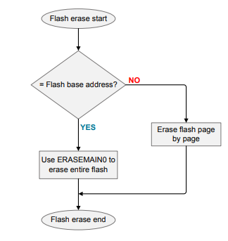
The flash base address of the Series 2 device is either 0x00000000 or 0x08000000. The timing for page erase or mass erase on each Series 2 device might vary. Refer to the device-specific datasheets for details.
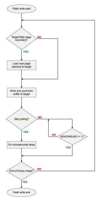
Flash Write#
The write operation requires that the address be written into the MSC ADDRB register. After each 32-bit word is written, the internal address register is incremented automatically by 4. When a word is written to the MSC WDATA register, the WDATAREADY bit of the MSC STATUS register is cleared. When this status bit is set, software can write the next word.
The flash program time (32-bit word) of each Series 2 device might vary. Refer to the device-specific datasheets for details.
To reduce the time for the flash write process, the program can omit polling the WDATAREADY bit in the MSC STATUS register after writing each 32-bit word, because the register read process is time consuming. The alternative is to add a fixed microseconds delay between each write to make sure the maximum write time can be met.
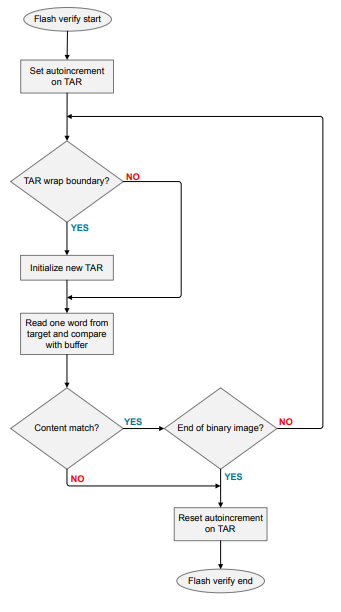
Flash Verify#
The program verifies the target flash contents with a buffer to make sure that no errors occurred during the programming process. The autoincrement of the Transfer Address Register (TAR) is for burst reads within the TAR wraparound boundary. The TAR must be initialized at every TAR wraparound boundary to set up the next flash read address.