Test Architecture and Equipment#
The following sections detail the recommended test architecture and equipment for each phase of testing, discuss test results and their dependence on test setup, and describe the typical manufacturing faults detected in manufacturing test.
Characterization Testing#
The architecture and test equipment used in the characterization stage of testing is more comprehensive than that of the volume manufacturing stages.
Test Architecture#
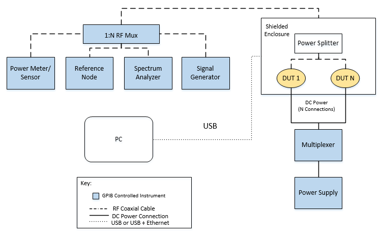
The following figure shows an example of the interfaces of the test equipment to the DUT. The test equipment can be controlled by test software through the General Purpose Interface Bus (GPIB) or Recommended Standard 232 (RS-232). The DUT may be controlled by utilizing the Wireless Starter Kit Mainboard which contains an on-board J-Link debugger and a Virtual COM port over USB or Ethernet, enabling application development and debugging/testing of custom hardware. For more information on the debug interfaces available, please refer to AN958: Debugging and Programming Interfaces for Custom Designs. Any number of DUTs may be tested at once, but this number is dependent on serial ports available and will affect the selection of the power splitter and matrix switch hardware described in the following figure.
Recommended Equipment#
The recommended characterization test setup uses Agilent test equipment for the basic radio frequency (RF) measurements and current measurements, as well as for supplying power to the DUT and switching the RF connections from the DUT to various types of measurement equipment. A Reference Node, as mentioned in the characterization stage of testing, is any Ember radio communication module (RCM) configured with the same radio chip as the DUT that can be used to verify transmission of packets from the DUT.
The following table lists the basic set of test equipment Silicon Labs has used for characterization testing. Please consult the equipment manufacturer for the appropriate models for these particular instruments.
Description | Purpose |
|---|---|
Power Meter | Used with power sensor to measure transmit power of the DUT |
Power Sensor | Used with power meter to measure transmit power of the DUT |
Universal Counter | Measures the transmission frequency offset of the DUT |
Spectrum Analyzer | Used to verify transmit power, Transmit Frequency Offset accuracy, and EVM of the DUT |
Signal Generator | Verifies reception of valid packets at the DUT |
Dual Output Power Supply | Powers the DUT and Reference Node |
Digital Multimeter | Verifies current consumption of the DUT in various modes of operation |
Data Acquisition Switch Unit | Supplies power to the DUT and switches RF connection |
3.5 GHz 1:N RF Mux Module | Switches RF connection from the DUT to the Reference Node/Spectrum Analyzer, frequency counter, power meter, or signal generator |
1:N Multiplexer Splitter | Splits power from test equipment to N DUTs; alternative parts can be used for more or fewer DUTs |
Shielded RF Enclosure | Provides RF isolation for the DUT during testing |
Reference Node | Known good radio module that is used as a receiver reference node in DUT transmit tests; manufacturer can be Silicon Labs, a Silicon Labs customer, or a Silicon Labs module partner |
Note: A power meter and frequency counter may be used in place of a spectrum analyzer in characterization testing to measure transmit power and transmit frequency offset. In volume manufacturing test, the power meter and frequency counter are a much more cost-effective method of measuring transmit power and transmit frequency offset than the spectrum analyzer.
Configuring Equipment#
Some test equipment needs to be configured specifically for 802.15.4/BLE radio communications. For the signal generator, for instance, the specific packet needs to be configured. Silicon Labs recommends contacting the specific test equipment manufacturer for information on configuring the signal generator for valid 802.15.4/BLE packets.
Low-Cost Alternative to Signal Generator (Golden Node)#
For some customers, adding a signal generator to manufacturing test is not desired or not possible due to cost concerns. In this case, Silicon Labs recommends using a Golden Node (a known good device that can be used in test for repeatable measurements) with TCXO (temperature controlled/compensated crystal oscillator). The TCXO allows for frequency accuracy when using the Golden Node as a known good transmitter source for DUT receive tests. Using a Golden Node without TCXO would present issues with test accuracy, as the crystal would drift over time and temperature. The Golden Node will have known transmitter performance (0 dBm +/0.5 dBm) across voltage and temperature, allowing for test repeatability.
RF Test Interface Examples#
The type of interface to the DUT and the RF shielded test enclosure selected for testing can determine the accuracy and repeatability of the measurements.
It is important to pay special attention to the RF test interface to the DUT because of the sensitivity of these signals. For example, a product with a 50-Ohm terminated Subminiature Type A (SMA) connector populated on the board can be connected directly to a coaxial cable with a known loss. Repeatability in this scenario is very good.
Another example is a product with an embedded antenna that was designed with test points for RF and ground can be connected with a pogo-pin style RF probe. The path loss from the RF test point to the cabled connections of the setup can be calibrated to determine accurate performance. The repeatability of this setup is dependent on the board layout, in the sense that the RF and ground signals should have test points in close proximity to one another. The repeatability is also more dependent on the shielded enclosure in this case, because the RF signal is exposed at the test point rather than enclosed within an SMA connector as in the first example.
As a final example, a product with an embedded antenna can be tested over the air within an enclosure. A reference antenna would be used within the enclosure to feed back the RF signal to the RF Mux. The path loss over the air from the reference antenna to the DUT antenna can be calibrated to determine accurate performance. Fixed position of the DUT and position of the DUT and reference antennas are crucial to getting repeatable results.
Low-Volume Manufacturing Testing#
The architecture and test equipment used in the characterization stage of testing is more comprehensive than that of the volume manufacturing stages.
Test Architecture#
The test architecture in the low-volume phase of testing is very similar to that of the characterization phase.
Recommended Equipment#
The equipment Silicon Labs recommends for the low-volume manufacturing phase of testing is very similar to that for the characterization phase. Some of the equipment may be removed depending on the tests selected for this phase.
Interference#
There are many RF devices in a test environment, such as wireless networks, microwave ovens, and mobile phones. For this reason, it is important to maintain RF isolation of the DUT from these sources of interference. It is also important to maintain RF isolation between multiple stations. For example, the equipment for test station A should be able to communicate only with a DUT from test station A and not with a DUT from test station B. Likewise, the equipment for test station B should be able to communicate only with a DUT from test station B and not a DUT from test station A. If these stations are not isolated from each other, the DUT will not be uniquely configured and multiple boards could share unique configuration information.
High-Volume Manufacturing Testing#
The architecture and test equipment used in the characterization stage of testing is more comprehensive than that of the volume manufacturing phases.
Test Architecture#
The test architecture in the high-volume phase of testing can be structured any number of ways depending on customer preference. One approach is to develop this test with a Golden Node programmed with an application that allows the DUT to obtain unique configuration information from the Golden Node through packets transmitted and received. This test may be limited to configuring one DUT at a time. The Golden Node initiates communication with the unconfigured DUT and sends unique configuration information to the DUT. The Golden Node can then interface with the PC application to configure the DUT uniquely. Then the DUT can reboot itself and be ready for testing or application operation. A basic transmit/receive test can then be run. The test architecture for this phase of testing is shown in the following figure.
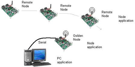
Another approach is to develop a test with a serial interface to both the Golden Node and the DUT. This may be more straightforward to develop but requires a more extensive set up and use of a UART.
Recommended Equipment#
The equipment is based on the tests selected for this phase of testing, as well as the preference of the customer. No matter the approach, it is important that, at the very least, the Golden Node (and in some cases the DUT) have an interface to a PC or server so that it can log test information like EUI, test results, and so on.
Interference#
A facility running multiple test stations maintains RF isolation among the stations, as previously detailed. In this test phase, the only interface to the DUT is power, as all communication between the Golden Node and the DUT is done through the radio. All of the test equipment used in the characterization testing can be removed from the process, unless a customer decides to continue to test certain functionality on the board that requires test equipment.
Manufacturing Coverage#
Manufacturing testing not only determines the tests that should be included in the manufacturing test phase, but it also helps detect manufacturing failures. The following sections provide some examples of typical manufacturing faults and how they are detected in testing.
IC Manufacturing#
Insufficient Solder on Ember IC#
An insufficient amount of solder will result in any number of failures in test. Insufficient solder will prevent some pins on the device from making contact with the pads on the board. This will result in programming failures, serial communication failures, and RF performance problems, all of which are detected in manufacturing test. Insufficient solder on the ground pad underneath the device will result in degraded RF performance, most likely in the receiver. This type of issue will be detected in either the Receive Waterfall Test or Receive Sensitivity Test. In some drastic cases where there is no solder on the ground pad and thus no ground connection from the device to the board, the device will not function and would either fail to program or fail to calibrate properly.
Wrong Component#
An incorrect component or component value will alter the performance of the board. For example, if a crystal tuning cap is the incorrect value, the Transmit Frequency Offset Test will detect this failure because the frequency will be outside the specified limits. If a component in the matching network is incorrect, this will affect the transmit power and will be detected in the Transmit Power Test. If a decoupling capacitor is the wrong value, it will affect the receiver performance of the device and will be detected in either the Receive Waterfall Test or the Receive Sensitivity Test.
Missing Component#
A missing component will also alter the performance of the board. For example, if there is a component missing from the RF path, there will be a major degradation in the transmit output power and overall receive sensitivity of the board. Also, if a component is missing that affects power distributed to the microprocessor or radio chips, the board will not be able to communicate serially in the case of the micro; the microprocessor will not configure the radio to transmit or receive in the case of the radio.
Solder Shorts or Opens#
A solder short or open on any component or device will cause any number of failures in manufacturing test. Any short or open in the RF circuitry of the board will cause degradation in performance and will be detected in various RF tests. A short or open in the DC circuitry or programming circuitry will prevent the device from programming properly and/or communicate properly with the test interface. For all of these cases mentioned, at least one test will detect a failure and flag this device as defective.
SiP Manufacturing#
SiP modules contain system-level components on a substrate inside a package and for this reason they require special guidance and considerations as part of a customer board manufacturing process. Refer to AN1223: LGA Manufacturing Guidance for module manufacturing guidance.