Generic Serial Peripheral Interface (GSPI) Architecture#
The Generic Serial Peripheral Interface (GSPI) on the SiWx917 is a high-performance, primary-only serial communication block.
It supports standard SPI protocols, Direct Memory Access (DMA), and power-efficient operation for high-throughput data exchange with SPI-compatible peripherals such as displays, sensors, and memory devices.
This section describes the GSPI architecture, functional blocks, operation modes, and software structure for integrating high-speed SPI communication in SiWx917-based applications.
Peripheral Overview#
The GSPI peripheral provides a dedicated synchronous serial primary that operates exclusively in Primary mode.
It supports full-duplex communication, enabling simultaneous data transmit and receive operations.
Key characteristics include:
Standard SPI protocol (Modes 0 and 3)
Programmable clock frequency and polarity/phase
16-entry TX/RX FIFOs
DMA interface for non-blocking transfers
Interrupt-driven event reporting
Three active-low chip-select signals (CS0–CS2)
Power-efficient operation in the high-performance (HP) domain
Functional Blocks#
The GSPI architecture includes several key functional components that work together to achieve efficient serial communication.
APB and DMA Interfaces#
Provide connectivity between the Cortex-M4 processor and the GSPI hardware.
The APB interface handles register access, while the DMA interface enables autonomous high-throughput data movement with minimal CPU load.
Transmit and Receive FIFOs#
Implement 16-entry deep TX and RX buffers to decouple the serial and system bus domains, increasing throughput and reducing latency.
Clock Generation and Control#
Generates the SPI clock (SCLK) with programmable divider, polarity, and phase control.
Supports Mode 0 and Mode 3 operation, with per-chip-select configuration.
Register Block#
Contains configuration, control, and status registers, such as:
GSPI_CONFIG1,GSPI_CONFIG2GSPI_STATUSFIFO threshold registers
These registers define frame format, clock configuration, and chip-select control.
Interrupt Controller#
Monitors FIFO thresholds, transfer completion, and error events.
Interrupts can be masked, cleared, or serviced through callbacks for event-driven operation.
Core Components#
Component | Description |
|---|---|
GSPI Primary | Dedicated SPI Primary providing high-speed, full-duplex serial communication |
DMA Interface | Enables non-blocking data transfers to/from memory |
FIFO Buffers | 16-entry TX and RX queues for efficient streaming |
Clock Generator | Programmable divider, polarity, and phase |
Chip Select Logic | Supports up to 3 active-low CSN outputs |
Interrupt Block | Signals transfer completion, FIFO thresholds, and error conditions |
Typical Use Cases#
GSPI is ideal for high-bandwidth or latency-sensitive devices such as:
Display controllers (LCD, OLED)
ADC/DAC converters
Audio codecs
Serial flash or EEPROM
Other microcontrollers
Functional Description#
The GSPI peripheral communicates over the Advanced Peripheral Bus (APB) and supports DMA for efficient data transfers.
It can operate in automatic or manual chip-select modes, providing flexibility for different device interfaces.
Block Diagram:
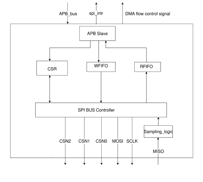
In manual mode, the application directly controls chip select and data timing for fine-grained operation.
Chip Select (CSN) Control#
GSPI_MANUAL_CSN_SELECT: Chooses the active chip select (CS0–CS2) in manual modeGSPI_MANUAL_CSN: Reflects the status of the selected CSN (0 = Active, 1 = Inactive)GSPI provides three active-low chip selects, allowing up to three SPI secondaries
Supported Operation Modes#
Serial Primary only: GSPI always acts as the SPI Primary and initiates all transfers.
Supported Protocols#
Supports standard SPI Protocols (Modes 0 and 3)
Frame size:
Manual mode: only 8 bit/16 bits (set by
GSPI_MANUAL_SIZE_FRM_REG)Or, specify 1–16 valid bits per frame via
GSPI_MANUAL_WRITE_DATA2
Full-duplex communication
Clock and timing control#
Use GSPI clocking and bus-mode registers to meet external device timing requirements:
Clock Divider: The 8-bit divider (
GSPI_CLK_DIV) derivesSCLKfrom the system clock.Gated SCLK: The clock toggles only during active transfers.
Per-CS Mode Control: Mode (0 or 3) is selectable per chip-select through
GSPI_BUS_MODE.Timing Profile: Configure
Full-speedorHigh-speedoperation inGSPI_BUS_MODE[0]before initiating transfers.
SPI Mode Timing (Frame-Format Reference)#
The GSPI supports SPI Mode 0 and Mode 3 frame formats.
Frame Length:
Configurable for 8-bit or 16-bit frames via GSPI_CONFIG2.
In manual mode, you can specify 1–16 valid bits per frame using GSPI_WRITE_DATA2.
Mode 0 (CPOL = 0, CPHA = 0)#
Idle clock: Low
Sample on rising edge
Data changes on falling edge

Mode 3 (CPOL = 1, CPHA = 1)#
Idle clock: High
Sample on falling edge
Data changes on rising edge

Note: Configured per chip select using the GSPI Bus Mode Register fields and the
GSPI_DATA_SAMPLE_EDGEbit.
Comparison Summary#
Parameter | Mode 0 | Mode 3 |
|---|---|---|
Idle SCLK Level | Low | High |
Sampling Edge | Rising | Falling |
Data Launch Edge | Falling | Rising |
SCLK Activity | Active only during data transfer |
Software Architecture#
This section describes the GSPI (Generic SPI) software architecture for the SiWx917 platform.
It explains how the software layers interact—from the application level down to the hardware—and provides guidance on structuring projects for portability, maintainability, and performance.
Layering Overview#
Although GSPI is a Primary-only peripheral, it follows the same layered software model used across other SiWx917 peripherals.
This unified structure promotes consistency, code reuse, and simplified maintenance across applications.
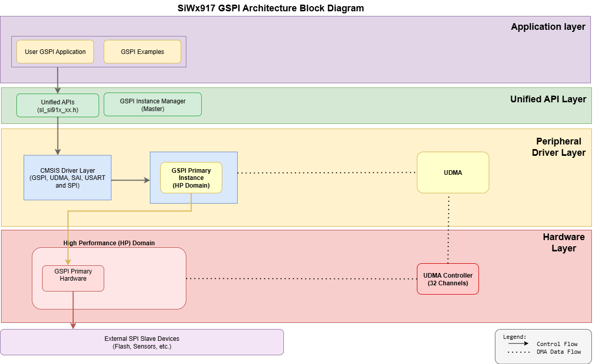
Figure: GSPI Software Layering and Interaction Model
Layer | Description |
|---|---|
Application Layer | Example projects (for example, |
Unified Driver Layer | High-level |
CMSIS Driver Layer | The Arm® CMSIS (Cortex Microcontroller Software Interface Standard) |
Peripheral Driver Layer | The low-level |
Hardware Layer | The physical GSPI hardware instance containing registers, FIFOs, clock generators, chip-select logic, data paths, DMA handshake signals, and interrupt/event sources. |
Note: The layered GSPI driver model ensures seamless migration between projects, easier debugging, and improved software scalability within the SiWx917 SDK.
Directory structure in WiSeConnect Software Development Kit (SDK)#
wiseconnect/
├── components/
│ └── device/
│ └── silabs/
│ └── si91x/
│ └── mcu/
│ └── drivers/
│ ├── cmsis_driver/
│ │ ├── CMSIS/Include/Driver_SPI.h
│ │ ├── GSPI.c
│ │ └── GSPI.h
│ ├── peripheral_drivers/
│ │ ├── inc/rsi_gspi.h
│ │ └── src/rsi_gspi.c
│ └── unified_api/
│ ├── inc/sl_si91x_gspi.h
│ └── src/sl_si91x_gspi.c
└── examples/
└── si91x_soc/
└── peripheral/
├── sl_si91x_gspi_basic
├── sl_si91x_gspi_dma
└── sl_si91x_gspi_manual_modeThis separation keeps applications independent of register-level details while still enabling optimized paths (for example, DMA plus low power) when needed.
Performance Modes#
The Generic SPI (GSPI) peripheral on the SiWx917 operates within the MCU High-Performance (HP) domain, which is powered by the performance clock tree.
The HP domain—including HP peripherals such as GSPI—is available only in PS4 and PS3 (Active) power states.
It is disabled in PS2, PS1, and PS0, including PS2-Sleep and Standby modes.
When the HP domain powers down, GSPI registers, FIFOs, and chip-select outputs lose their state.
You must reinitialize GSPI after wake-up to restore functionality.
Speed and Timing Modes#
Select a timing profile that best balances throughput, signal integrity, and power consumption for your system.
1. Full-Speed Mode#
SCLK range: 0 – 58 MHz (max)
Edge relationship: Launch data on the negative edge, sample on the positive edge
Recommended for: Most peripheral devices and standard PCB trace lengths
2. High-Speed Mode#
SCLK range: 58 – 116 MHz (max)
Edge relationship: Negative edge driving and negative edge sampling (tightened setup/hold timing)
Recommended for: High-speed peripherals when signal quality and timing margins have been verified
Tip: For long traces or noisy environments, use full-speed mode to maintain reliable signal integrity.
Dependencies#
The GSPI peripheral requires a combination of hardware pins and software components for operation.
This section outlines the required dependencies for both hardware and software.
Hardware Dependencies#
Component | Purpose |
|---|---|
GPIO Primary | Configures SCLK, chip-select (CSN0–CSN3), and data lines. Common naming follows SPI conventions: MOSI (Master Out / Slave In) and MISO (Master In / Slave Out). |
DMA Controller | Provides high-throughput, non-blocking data transfers. |
Peripheral Clock and PMU | Manages clock gating and power domains for the HP subsystem. |
Note: Verify that GSPI-related GPIOs are correctly routed and that the DMA controller is enabled if using DMA-assisted transfers.
Software Dependencies#
Software Component | Purpose |
|---|---|
| Core GSPI driver for initialization, configuration, manual mode control, and data transfer. |
| General-purpose I/O driver for pin multiplexing and routing. |
| DMA driver (optional) for continuous or large data transfers. |
Clock and Power Drivers | Manage peripheral clock enables and low-power state transitions. |
Tip: Simplicity Studio automatically manages these dependencies when you add the GSPI component through the Project Configurator and Universal Configurator (UC).
Integration and Configuration Workflow#
For a complete setup guide—including Simplicity Studio configuration, UC parameter setup, and code generation, see the
GSPI Initialization and Configuration Guide.