SPI Features and Configurations#
SPI Signals#
SiWx917 NCP mode (SiWN917) supports only the SPI secondary interface. SiWN917 detects the host interface automatically after connecting to respective host controllers like SDIO, SPI, UART, USB and USB-CDC. SPI interfaces are detected through hardware packet exchanges.
The following section provides signal descriptions for the SPI interface. For more details about the pin names and descriptions, please refer to the SiWx917 data sheet.
| SPI Signals | Supply Domain | Direction | Initial State (Power-up, Active Reset & Sleep State) | Description (All signals are in default states unless otherwise mentioned) |
|---|---|---|---|---|
| SPI_CLK | SDIO_IO_VDD | Input | High-Z | Serial Clock Input |
| SPI_CSN | SDIO_IO_VDD | Input | High-Z | Active-low Chip Select signal initiated by the main device to select a secondary device |
| SPI_MOSI | SDIO_IO_VDD | Input | High-Z | Main-Out-Secondary-In signal for data transfer from main device to secondary device |
| SPI_MISO | SDIO_IO_VDD | Output | High-Z | Main-In-Secondary-Out signal for data transfer from Secondary to main device |
| SPI_INTR | SDIO_IO_VDD | Output | High-Z | Interrupt signal to main device for indicating that the data is available with the Secondary device. Upon interrupt, main device must initiate SPI transaction and read the available data on the SPI_MISO line. For more details about this signal, read the below 'Note' section. |
| SPI_ERR_INTR | SDIO_IO_VDD | Output | Initial State: Pull-up; Sleep State: High-Z | This signal is not available in the Default state. Check its availability in the Software. If SPI core logic within the device has gone to a state where it is not able to recover and process SPI transactions from the external main device, then SPI_ERR_INTR is asserted to the external main device about this status. It is an active high output signal. Once this signal is asserted by the devices, then the external host must initialize SPI and start the transactions again. |
Note:
Default state refers to the state of the device after initial boot loading and firmware loading is complete.
Sleep state refers to the state of the device after entering Sleep state which is indicated by Active-High
SLEEP_IND_FROM_DEVsignal.Refer to the WiSeConnect API Reference Guide for software programming information in embedded mode.
Ensure that the input signals SPI_CSN and SPI_CLK are not floating when the device is powered up and reset is de- asserted. This can be done by ensuring that the host processor configures its signals (outputs) before de-asserting the reset. SPI_INTR is the interrupt signal driven by the secondary device. This signal may be configured as Active- high or Active-low. If it is active-high, an external pull-down resistor may be required. If it is active-low, an external pull-up resistor may be required. This resistor can be avoided if the following action needs to be carried out in the host processor.
To use the signal in active-high or active-low mode, ensure that during the power-up of the device the interrupt is disabled in the host processor before de-asserting the reset. After de-asserting the reset, the interrupt needs to be enabled only after the SPI initialization is done, and the interrupt mode is programmed to either active-high or active-low mode as required.
The host processor needs to disable the interrupt before the ULP Sleep mode is entered and enable it after the SPI interface is reinitialized upon wakeup from ULP Sleep.
SPI Modes#
The following table lists the four SPI modes:
| SPI Mode | Clock Polarity (CPOL) | Clock Phase (CPHA) | Clock Idle | Sample Edge | Shift Edge |
|---|---|---|---|---|---|
| 0 | 0 | 0 | Low | Data is sampled on the rising edge of the clock | Data is driven on falling edge |
| 1 | 0 | 1 | Low | Data is sampled on falling edge of the clock | Data is driven on rising edge |
| 2 | 1 | 0 | High | Data is sampled on falling edge of the clock | Data is driven on rising edge |
| 3 | 1 | 1 | High | Data is sampled on the rising edge of the clock | Data is driven on falling edge |
Note: SiWN917 supports Mode 0 only. There is no API available for changing the mode.
The following figure illustrates mode-0. The data is shown on the MOSI and MISO lines. The start and end of transmission is indicated by the dotted green line, the sampling edge is indicated in orange, and the shifting edge is indicated in blue.
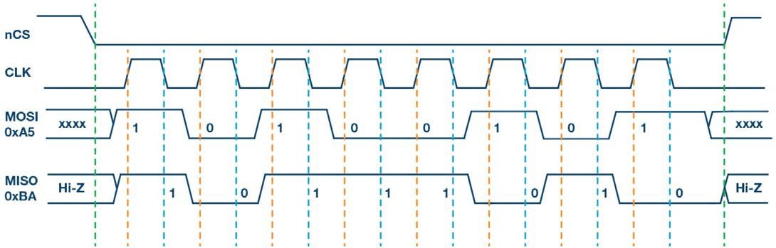
Note: For high-speed mode, the SiWN917 has a special custom design to drive the data on the rising edge (a half cycle earlier), which usually happens at falling edge as per Mode 0, while still meeting the SPI protocol specifications. This is not a new SPI mode (data is driven on the rising edge and sampled on the rising edge), but an enhancement, when SiWN917 is in high-speed mode.
SPI Transactions Logic Capture#
In this section, SPI transactions between SiWN917 and EFR32xG21 MCU are captured using Logic Software. The following are the setup instructions for SPI protocol in 'Logic software'.
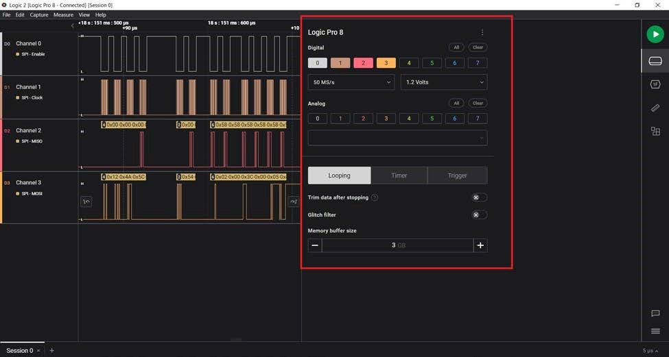
Connect the Saleae Logic analyzer pins with the SPI pins on the host MCU for SPI logic capture.
Open the Logic software and click on the Device Settings tab towards the right side of the Logic software screen and select the Digital channels that are connected with Saleae Logic Analyzer.
Select the sampling rate. This must be greater than the SPI clock frequency being used by host MCU for communication with SiWN917 (generally, the higher the better).
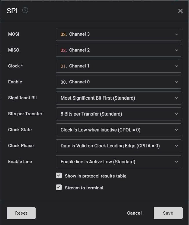
Now click on Analyzers tab towards the right side of the screen and select 'SPI'.
A new 'SPI' window is opened. Select the corresponding channels for SPI MOSI, MISO, Clock, and Enable.
Select Most Significant Bit First as the significant bit, clock state as CPOL = 0 and clock phase as CPHA = 0. Other settings must be made as per the following image.
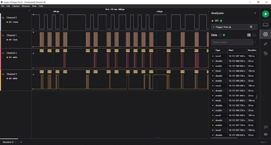
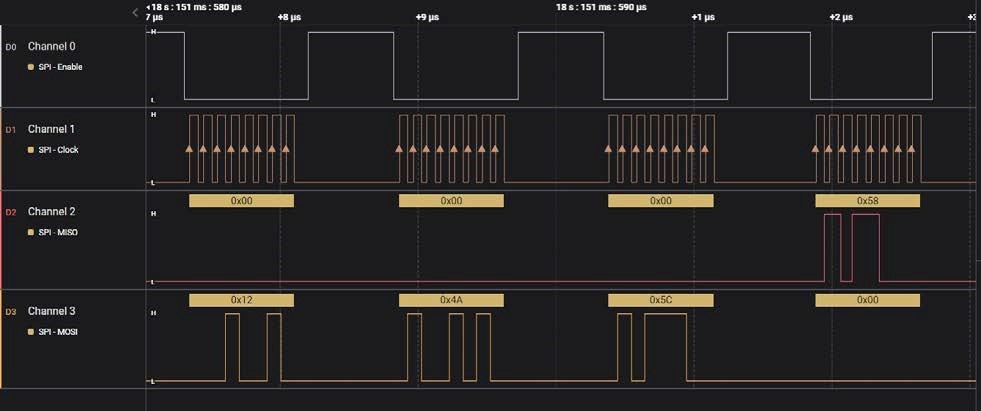
Once the above setup is complete, one should see the SPI transactions in the Logic Software as soon as an SiWx917 Wi-Fi/BLE application is run and the Play button is clicked in Logic software. These transactions should look like the following:
Notes:
To be precise, the above SPI transactions can be captured when
sl_net_init()API (defined in thewiseconnect/components/service/network_managersub-component of the WiSeConnect SDK) is run. Driver initialization, device initialization, and wireless initialization happen within this API. As an out-of-box experience, users can run any default WiSeConnect example from the SDK folder,wiseconnect/examples/featuredorwiseconnect/examples/snippetswhere this API is called in the corresponding'app.c'file of the application.Before running an application, users must ensure they successfully port the WiSeConnect SDK Hardware Abstraction Layer (HAL) to the host MCU in use. For more information on HAL porting, refer to SiWx91x NCP WiSeConnect SDK Porting Guide. The SDK is already ported to EFx32 family of MCUs and the corresponding HAL can be found in
wiseconnect/components/si91x/platforms/efx32.With EFx32 as the host MCU, the host SPI interface is brought-up with 12.5 MHz SPI clock frequency (Check the baud rate in the definition of
sl_si91x_host_usart2_init()API present in the file,wiseconnect/components/si91x/platforms/efx32/efx32_ncp_host_spi.c). To enable high-speed mode, the user has to implement thesl_si91x_host_enable_high_speed_bus()API for the host MCU in use as part of the HAL porting. For EFx32, this has been implemented (definition can be found inefx32_ncp_host_spi.cfile). Note that SiWx917 host SPI interface supports host SPI clock frequencies up to 100 MHz.
SPI Log Decoding Guide#
The SPI transaction flow between SiWN917 and the host MCU is described in this section. The following are captures of the SPI transfers after a module hardware reset.
Enabling High-Speed SPI#
SPI transfers with clock frequencies up to 25 MHz are termed low-speed transmissions, and during these transmissions, data is driven on the falling edge of the clock and sampled on the rising edge of the clock. Transmissions above 25 MHz are termed high-speed transmissions, and during these transmissions, data is driven on the rising edge of the clock and sampled on the falling edge of the clock. SiWN917 SPI interface also supports Ultra High-Speed mode, with clock frequencies reaching up to 100 MHz. SPI initialization is done in low-speed mode. After initialization, to enable high-speed mode, the following SPI transactions take place:
| MOSI Byte Explained (Tx to Module) | MOSI | MISO | MISO Byte Explained (Tx to Host MCU) | Other Possibilities |
|---|---|---|---|---|
| Register Write | 0x62 | 0x00 | Dummy data | |
| SPI Register’s address | 0x08 | 0x58 | Success token | |
| 0x00 | 0x58 | Success token | 0x52, 0x54 | |
| Write ‘0x03’ for enabling high speed SPI | 0x03 | 0x00 | Dummy data | 0x07 – Ultra High-Speed Mode (100 MHz) |
Wait for CARD READY from the module. This the first message that is read during wireless initialization.
Note: When an incorrect firmware is loaded onto the module, say chip version - 1.5 firmware is loaded on a 1.4 chipset, the BOARD_READY message will be sent by the module but no CARD_READY message will be sent to the host.
The Interrupt Status Register's (ISR) value is read before performing a frame read or frame write. Whenever the module sends data or a response to the host MCU, the register holds the value of 0x08. Whenever the host MCU wants to send or write a command frame to the module, the register holds the value of 0x00.
| MOSI Byte Explained (Tx to Module) | MOSI | MISO | MISO Byte Explained (Tx to Host MCU) | Other Possibilities |
|---|---|---|---|---|
| Register Read | 0x41 | 0x00 | Dummy data | — |
| RSI_SPI_INT_REG_ADDR Register Address | 0x00 | 0x58 | Success token | 0x52, 0x54 |
| Dummy data | 0x00 | 0x55 | Start token | — |
| Dummy data | 0x00 | 0x08 | Module to send data to host | — |
| Pre-frame descriptor read | 0x5C | 0x00 | Dummy data | — |
| 8-bit mode | 0x00 | 0x58 | Success token | 0x52, 0x54 |
| LSB of the number of bytes to be read (read first 4 bytes of the pre-frame descriptor) | 0x04 | 0x58 | Success token | 0x52, 0x54 |
| MSB of the number of bytes to be read | 0x00 | 0x58 | Success token | 0x52, 0x54 |
| Dummy data | 0x00 | 0x58 | Success token for memory read | 0x52, 0x54 |
| Dummy data | 0x00 | 0x55 | Start token followed by four bytes | — |
| Dummy data | 0x00 | 0x14 | 0x14– 0x04 = 16 bytes are to be read from the module | — |
| Dummy data | 0x00 | 0x00 | — | |
| Dummy data | 0x00 | 0x04 | — | |
| Dummy data | 0x00 | 0x00 | — | |
| Frame Read | 0x5D | 0x00 | Dummy data | — |
| 8-bit mode | 0x00 | 0x58 | Success token | 0x52, 0x54 |
| LSB of the number of bytes to be read | 0x10 | 0x58 | Success token | 0x52, 0x54 |
| MSB of the number of bytes to be read | 0x00 | 0x58 | Success token | 0x52, 0x54 |
| Dummy data | 0x00 | 0x58 | Success token | 0x52, 0x54 |
| Dummy data | 0x00 | 0x55 | Start token | — |
| Dummy data | 0x00 | 0x00 | Payload length = 0 | — |
| Dummy data | 0x00 | 0x40 | 4 – Management Packet | — |
| Dummy data | 0x00 | 0x89 | 0x89 – Command ID for CARD READY | — |
| Dummy data | 0x00 | 0x00 | — | — |
| Dummy data | 0x00 | 0x00 | — | — |
| Dummy data | 0x00 | Ten dummy bytes | — | — |
| Dummy data | 0x01 | Ten bytes of zeros | — | — |
After the CARD READY message, every instruction or command is sent to the module via the Frame Write operation, and the response from the module is read via the Frame Read operation. Hence, these commands are termed Command frames.
Any command frame that is transferred between host and the module consists of Management frame (which constitutes the data payload length, management packet, and command ID) and data frame. Management frames are used to configure the Wi-Fi module to access Wi-Fi connectivity, TCP/IP stack, etc. Data frames are used to transfer the data.
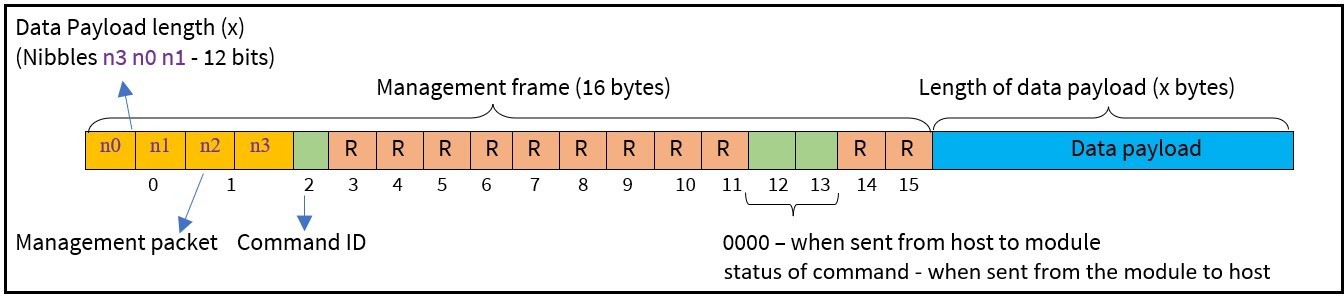
The data payload length can be known from the nibbles – n3 n0 n1 (with n3 being the most significant nibble) and should be retrieved in that order. For example, if the values of n0 n1 n2 n3 are 7 d 4 5 respectively, then the data payload length is (n3 n0 n1), i.e., 0x57d (1405 bytes).
The 'n2' nibble determines the management packet.
Every command frame has its own command ID.
SPI Initialization#
The SPI initialization process takes place during device initialization. The host MCU needs to initialize SPI to communicate with SiWN917. This is done by transmitting 0x12, 0x4A, 0x5C, 0x00 on the MOSI line. After successful SPI initialization, SiWN917 sends a success token, i.e., 0x58 on MISO line.
MOSI:0x12 0x4A 0x5C 0x00MISO:0x00 0x00 0x00 0x58 (Successful SPI Initialization)
Note: If your application requires SPI clock frequency greater than 25 MHz, the host must initialize the SPI interface with a clock frequency less than or equal to 25 MHz. Post SPI initialization, all the other SPI transactions can be carried out at a clock frequency greater than 25 MHz. This functionality is to be implemented while porting WiSeConnect SDK to your host application. Refer to Porting for an External Host guide.
Before going further, it is necessary to note the following SPI tokens sent by SiWN917 over MISO:
0x58- Success response
0x52- Failure response
0x54- Busy response (a new transaction is initiated while the previous transaction's response is still pending from the module)
0x55- Start token (Module is ready to transmit data)
Recommendation- Use a SPI cable of less than 2 inches length for prototyping.
If the SPI cable is not connected properly between the host and SiWN917, the host MCU waits for the response from the module for some reasonable time and throws
SL_STATUS_SPI_BUSYerror (with error code:0x0054) for device initialization.
SiWN917 Initialization Transactions#
BOARD READY: After successful initialization of the SPI interface with the module, the first message checked by the host is BOARD READY from the module. If the bootup options integrity passes, the RSI_HOST_INTF_REG_OUT register contains 0xABxx where 'xx' represents the two-nibble bootloader version.
CARD READY: After the firmware gets loaded onto the module successfully, CARD READY is the first message from the loaded firmware that is sent to the Host MCU.
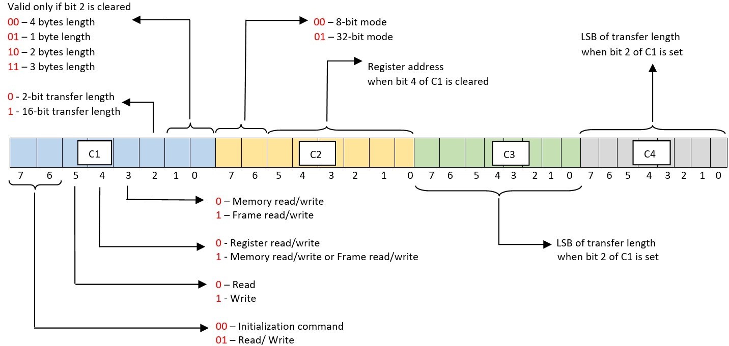
The SPI interface is programmed to perform transfers using commands C1, C2, C3 and C4 and an optional 32-bit address (sent during register read/write or memory read/write).
After successful initialization of the SPI interface, the host waits for BOARD READY from the module. For checking the BOARD READY from the module, the host reads the contents of RSI_HOST_INTF_REG_OUT register of module with LSB of address transmitted first.
| MOSI Byte Explained (Tx to Module) | MOSI | MISO | MISO Byte Explained (Tx to Host MCU) | Other Possibilities |
|---|---|---|---|---|
| Memory Read | 0x54 | 0x00 | Dummy data | — |
| 8-bit Mode | 0x00 | 0x58 | Success token | 0x52, 0x54 |
| LSB of the length of data to be read — Two bytes | 0x02 | 0x58 | Success token | 0x52, 0x54 |
| MSB of the length of data to be read | 0x00 | 0x58 | Success token | 0x52, 0x54 |
| RSI_HOST_INTF_REG_OUT — Address to be read (LSB first) | 0x3C | 0x58 | Success token for Memory Read | 0x52, 0x54 |
| 0x00 | 0x58 | Success token | 0x52, 0x54 | |
| 0x05 | 0x58 | Success token | 0x52, 0x54 | |
| 0x41 | 0x58 | Success token | 0x52, 0x54 | |
| Dummy data | 0x00 | 0x58 | Success token | 0x52, 0x54 |
| Dummy data | 0x00 | 0x55 | Start token followed by two bytes of data | 0x52, 0x54 |
| Dummy data | 0x00 | 0x11 | Bootloader version 1.1 | 0x10 — Bootloader version 1.0 |
| Dummy data | 0x00 | 0xAB |
HOST_INTERFACE_REG_OUT_VALID (0xAB11 or 0xAB10 indicates that the bootloader integrity check is passed. This is named as ‘BOARD READY’ message) |
• 0xABF1 — indicates that the last configuration of bootup options is not saved • 0xABF2 — indicates that the bootup options checksum failed |
Before checking the CARD READY from the module, the host needs to check whether the Interrupt signals are active low or active high. This can be known from the contents of RSI_INT_MASK_REG_ADDR register (at address 0x41050000) of module by performing memory read to that address.
| MOSI Byte Explained (Tx to Module) | MOSI | MISO | MISO Byte Explained (Tx to Host MCU) | Other Possibilities |
|---|---|---|---|---|
| Memory Read | 0x54 | 0x00 | Dummy data | — |
| 8-bit Mode | 0x00 | 0x58 | Success token | 0x52, 0x54 |
| LSB of the length of data to be read - Two bytes | 0x02 | 0x58 | Success token | 0x52, 0x54 |
| MSB of the length of data to be read | 0x00 | 0x58 | Success token | 0x52, 0x54 |
| RSI_INT_MASK_REG_ADDR Address to be read (LSB first) | 0x00 | 0x58 | Success token for Memory Read | 0x52, 0x54 |
| 0x00 | 0x58 | Success token | 0x52, 0x54 | |
| 0x05 | 0x58 | Success token | 0x52, 0x54 | |
| 0x41 | 0x58 | Success token | 0x52, 0x54 | |
| Dummy data | 0x00 | 0x58 | Success token | 0x52, 0x54 |
| Dummy data | 0x00 | 0x55 | Start token followed by two bytes of data | 0x52, 0x54 |
| Dummy data | 0x00 | 0x00 | LSB of the Register | 0x52, 0x54 |
| Dummy data | 0x00 | 0x01 | MSB of the Register (0x02– Active Low Interrupts) | 0x52, 0x54 |
For ACTIVE HIGH INTERRUPTS, write ‘0x00’ into RSI_INT_MASK_REG_ADDR (at address 0x41050000) register of the module.
| MOSI Byte Explained (Tx to Module) | MOSI | MISO | MISO Byte Explained (Tx to Host MCU) | Other Possibilities |
|---|---|---|---|---|
| Memory Write | 0x74 | 0x00 | Dummy data | — |
| 8-bit Mode | 0x00 | 0x58 | Success token | 0x52, 0x54 |
| LSB of the size of the memory into which data must be written – Two bytes | 0x02 | 0x58 | Success token | 0x52, 0x54 |
| MSB of the size of the memory into which data must be written | 0x00 | 0x58 | Success token | 0x52, 0x54 |
| RSI_INT_MASK_REG_ADDR Address (LSB first) | 0x00 | 0x58 | Success token for Memory write command | 0x52, 0x54 |
| 0x00 | 0x58 | Success token | 0x52, 0x54 | |
| 0x05 | 0x58 | Success token | 0x52, 0x54 | |
| 0x41 | 0x58 | Success token | 0x52, 0x54 | |
| LSB to be written | 0x00 | 0x58 | Success token | 0x52, 0x54 |
| MSB to be written (0x00 – Active High Interrupts) | 0x00 | 0x58 | Success token | MSB = 0x02 – when opted for Active Low Interrupts during device initialization |
Write LOADFIRMWARE instruction into RSI_HOST_INTF_REG_OUT register (at address 0x4105003C) and ‘RSI_HOST_INTF_REG_IN register (at address 0x41050034) of the module.
| MOSI Byte Explained (Tx to Module) | MOSI | MISO | MISO Byte Explained (Tx to Host MCU) | Other Possibilities |
|---|---|---|---|---|
| Memory Write | 0x74 | 0x00 | Dummy data | — |
| 8-bit Mode | 0x00 | 0x58 | Success token | 0x52, 0x54 |
| LSB of the size of the memory into which data must be written – Two bytes | 0x02 | 0x58 | Success token | 0x52, 0x54 |
| MSB of the size of the memory into which data must be written | 0x00 | 0x58 | Success token | 0x52, 0x54 |
| RSI_HOST_INTF_REG_OUT Address (LSB first) | 0x3C | 0x58 | Success token for Memory write command | 0x52, 0x54 |
| 0x00 | 0x58 | Success token | 0x52, 0x54 | |
| 0x05 | 0x58 | Success token | 0x52, 0x54 | |
| 0x41 | 0x58 | Success token | 0x52, 0x54 | |
| LSB to be written | 0x00 | 0x58 | Success token | 0x52, 0x54 |
| MSB to be written (Write ‘0’ into RSI_HOST_INTF_REG_OUT Register) | 0x00 | 0x58 | Success token | MSB = 0x02 – when opted for Active low interrupts during device initialization |
| Memory Write | 0x74 | 0x00 | Dummy data | — |
| 8-bit Mode | 0x00 | 0x58 | Success token | 0x52, 0x54 |
| LSB of the size of the memory into which data must be written – Two bytes | 0x02 | 0x58 | Success token | 0x52, 0x54 |
| MSB of the size of the memory into which data must be written | 0x00 | 0x58 | Success token | 0x52, 0x54 |
| RSI_HOST_INTF_REG_IN Address (LSB first) | 0x34 | 0x58 | Success token for Memory write command | 0x52, 0x54 |
| 0x00 | 0x58 | Success token | 0x52, 0x54 | |
| 0x05 | 0x58 | Success token | 0x52, 0x54 | |
| 0x41 | 0x58 | Success token | 0x52, 0x54 | |
| LSB to be written (Load default firmware with ACTIVE HIGH interrupts) | 0x31 | 0x00 | Dummy data | 0x71 – Load default firmware with ACTIVE LOW interrupts |
| MSB to be written (RSI_HOST_INTERACT_REG_OUT Register) | 0xAB | 0x00 | Dummy data | |
| Memory Read | 0x54 | 0x58 | Success token for memory write | 0x52, 0x54 |
| 8-bit Mode | 0x00 | 0x58 | Success token | 0x52, 0x54 |
| LSB of the length of data to be read - Two bytes | 0x02 | 0x58 | Success token | 0x52, 0x54 |
| MSB of the length of data to be read | 0x00 | 0x58 | Success token | 0x52, 0x54 |
| RSI_HOST_INTF_REG_OUT Address (LSB first) | 0x3C | 0x58 | Success token | 0x52, 0x54 |
| 0x00 | 0x58 | Success token | 0x52, 0x54 | |
| 0x05 | 0x58 | Success token | 0x52, 0x54 | |
| 0x41 | 0x58 | Success token | 0x52, 0x54 | |
| Dummy data | 0x00 | 0x58 | Success token | 0x52, 0x54 |
| Dummy data | 0x00 | 0x55 | Start token | 0x52, 0x54 |
| Dummy data | 0x00 | 0xAA | RSI_CHECKSUM_SUCCESS | 0x23 – When valid firmware is not present and device initialization fails. |
| Dummy data | 0x00 | 0xAB | RSI_HOST_INTERACT_REG_OUT_VALID | 0x52, 0x54 |
For more information on the boot results, refer to the header file,
components/si91x/inc/sl_si91x_constants.h.
Enabling High Speed SPI#
SPI transfers with clock frequencies up to 25 MHz are termed low-speed transmissions, and during these transmissions, data is driven on the falling edge of the clock and sampled on the rising edge of the clock. Transmissions above 25 MHz are termed high-speed transmissions, and during these transmissions, data is driven on the rising edge of the clock and sampled on the falling edge of the clock. The SiWN917 SPI interface also supports Ultra High-Speed mode, with clock frequencies reaching up to 100 MHz. SPI initialization is done in low-speed mode. After initialization, to enable high-speed mode, the following SPI transactions take place:
| MOSI Byte Explained (Tx to Module) | MOSI | MISO | MISO Byte Explained (Tx to Host MCU) | Other Possibilities |
|---|---|---|---|---|
| Register Write | 0x62 | 0x00 | Dummy data | |
| SPI Register’s address | 0x08 | 0x58 | Success token | |
| 0x00 | 0x58 | Success token | 0x52, 0x54 | |
| Write ‘0x03’ for enabling high speed SPI | 0x03 | 0x00 | Dummy data | 0x07 – Ultra High-Speed Mode (100 MHz) |
Wait for CARD READY from the module. This the first message that is read during wireless initialization.
Note: When an incorrect firmware is loaded onto the module, say chip version - 1.5 firmware is loaded on a 1.4 chipset, the BOARD_READY message will be sent by the module but not CARD_READY message will be sent to the host.
The Interrupt Status Register's (ISR) value is read before performing a frame read or frame write. Whenever the module sends data or a response to the host MCU, the register holds the value of 0x08. Whenever the host MCU wants to send or write a command frame to the module, the register holds the value of 0x00.
| MOSI Byte Explained (Tx to Module) | MOSI | MISO | MISO Byte Explained (Tx to Host MCU) | Other Possibilities |
|---|---|---|---|---|
| Register Read | 0x41 | 0x00 | Dummy data | - |
| RSI_SPI_INT_REG_ADDR Register Address | 0x00 | 0x58 | Success token | 0x52, 0x54 |
| Dummy data | 0x00 | 0x55 | Start token | |
| Dummy data | 0x00 | 0x08 | Module to send data to host | |
| Pre-frame descriptor read | 0x5C | 0x00 | Dummy data | |
| 8-bit mode | 0x00 | 0x58 | Success token | 0x52, 0x54 |
| LSB of the number of bytes to be read (read first 4 bytes of the pre-frame descriptor) | 0x04 | 0x58 | Success token | 0x52, 0x54 |
| MSB of the number of bytes to be read | 0x00 | 0x58 | Success token | 0x52, 0x54 |
| Dummy data | 0x00 | 0x58 | Success token for memory read | 0x52, 0x54 |
| Dummy data | 0x00 | 0x55 | Start token followed by four bytes | |
| Dummy data | 0x00 | 0x14 | 0x14 – 0x04 = 16 bytes are to be read from the module | |
| Dummy data | 0x00 | 0x00 | ||
| Dummy data | 0x00 | 0x04 | ||
| Dummy data | 0x00 | 0x00 | ||
| Frame Read | 0x5D | 0x00 | Dummy data | |
| 8-bit mode | 0x00 | 0x58 | Success token | 0x52, 0x54 |
| LSB of the number of bytes to be read | 0x10 | 0x58 | Success token | 0x52, 0x54 |
| MSB of the number of bytes to be read | 0x00 | 0x58 | Success token | 0x52, 0x54 |
| Dummy data | 0x00 | 0x58 | Success token | 0x52, 0x54 |
| Dummy data | 0x00 | 0x55 | Start token | |
| Dummy data | 0x00 | 0x00 | Payload length = 0 | |
| Dummy data | 0x00 | 0x40 | 4 – Management Packet | |
| Dummy data | 0x00 | 0x89 | 0x89 – Command ID for CARD READY | |
| Dummy data | 0x00 | 0x00 | ||
| Dummy data | 0x00 | 0x00 | ||
| Dummy data | 0x00 | 0x01 | ||
| Dummy data | Ten dummy bytes | Ten bytes of zeros |
After the CARD READY message, every instruction or command is sent to the module via the 'Frame Write' operation, and the response from the module is read via the 'Frame Read' operation. Hence, these commands are termed Command frames.
Any command frame that is transferred between host and the module consists of Management frame (which constitutes the data payload length, management packet, and command ID) and data frame. Management frames are used to configure the Wi-Fi module to access Wi-Fi connectivity, TCP/IP stack etc. Data frames are used to transfer the data.
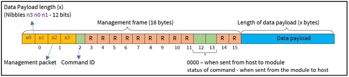
The data payload length can be known from the nibbles – n3 n0 n1 (with n3 being the most significant nibble) and should be retrieved in that order. For example, if the values of n0 n1 n2 n3 are 7 d 4 5 respectively, then the data payload length is (n3 n0 n1), i.e., 0x57d (1405 bytes).
The 'n2' nibble determines the management packet.
Every command frame has its own command ID.