Matching Circuit#
The PA of the transmitter should be matched for maximum power transfer and the LNA of the receiver must be matched for best sensitivity. The matching is divided into the following operations:
Matching the SoC transceiver to a 50 RF line on the PCB.
Matching the 50 RF line of the PCB to the antenna.
The first part is already done in the ZGM230S SiP and is therefore only applicable to the EFR32ZG23. The second part must be done for all implementations unless a naturally matched antenna is used.
Summary of Matching Networks#
The recommended matching networks for general Z-Wave and Z-Wave long range are shown in the table below:
| General Z-Wave | Z-Wave Long Range | ||||
|---|---|---|---|---|---|
| EFR32ZG23 | ZGM230S | EFR32ZG23 | ZGM230S | ||
| 14 dBm | 14 dBm | 14 dBm | 20 dBm | 14 dBm | |
| Matching w/o SAW |
|
No external match needed (BRD4205B) |
|
|
No external match needed (BRD4205B) |
| Matching w/SAW |
|
SAW in TX/RX path |
|
|
SAW in TX/RX path |
| Max. power for US | -1 dBm | -1 dBm | 14 dBm | 20 dBm | 14 dBm |
| Max. power for EU | 14 dBm | 14 dBm | N/A | N/A | N/A |
The matching network solutions listed above are detailed below.
SoC to RF Line Matching#
EFR32ZG23 | ZGM230S |
|---|---|
Applicable | N/A |
The EFR32ZG23 antenna interface consists of two single-ended input pins (SUBG_I0 and SUBG_I1) that interface directly to two LNAs and two single-ended output pins that interface directly to two +14 dBm or +20 dBm PAs (SUBG_O0 and SUBG_O1). Integrated switches select either SUBG_O0 or SUBG_O1, SUBG_I0, or SUBG_I1 to be the active paths.
Note: The Z-Wave gateway or end-device FW for EFR32ZG23 delivered as part of the Z-Wave SDK enables RF interface 0 only. Therefore, only SUBG_O0 and SUBG_I0 can be used as active ports on EFR32ZG23 when using the Z-Wave gateway or end-device FW.
EFR32ZG23 parts are available either with the +14 dBm (LPA) or +20 dBm (HPA) Class-D PAs. These are internally bonded options, so different OPN part numbers are used for the chip variants with different maximum TX power levels.
The typical RF impedance matching network topology for EFR32ZG23 is shown in the figure below, where all components do not need to be populated but different BOM options are required for different output power level requirements (14 or 20 dBm). Series dc-blocking capacitor of C5 in the TX path is required, while dc decoupling in the RX path is not needed. The unused RF ports should be left float-ing, i.e., terminated with an open load.
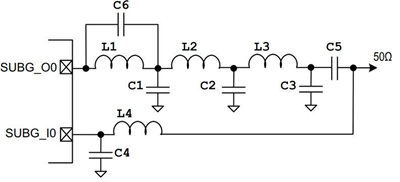
The TX matching network includes the low-pass filtering function as well to suppress the TX harmonics, while the RX matching network provides the highest possible voltage gain to the LNA by transforming the impedance up while the LNA capacitance is resonated out. The table below provides a summary of the matching component values versus output power.
P_OUT | PAVDD | L1 | L2 | L3 | L4 | C1 | C2 | C3 | C4 | C5 | C6 |
|---|---|---|---|---|---|---|---|---|---|---|---|
14 dBm | 1.8 V | 4.2 nH | 16 nH | 0R | 18 nH | 5.9 pF | 2.1 pF | N.M. | N.M. | 220 pF | N.M. |
20 dBm | 3.3 V | 1.5 nH | 1.3 nH | 13 nH | 18 nH | N.M. | 7.2 pF | 1.3 pF | N.M. | 220 pF | 1.9 pF |
Using a SAW filter on Z-Wave 800 devices is possible and in some cases strongly recommended. SAW filter component specifications can be found in Component Specifications. As shown in Summary of Matching Networks, the recommended configuration of the SAW filter for EFR32ZG23 devices is to add that to the RX path only to avoid the decreased TX power due to the SAW filter insertion loss in TX path. More details about how to implement SAW filter on EFR32ZG23 devices can be found in [14].
RF Line to Antenna Matching#
EFR32ZG23 | ZGM230S |
|---|---|
Applicable | Applicable |
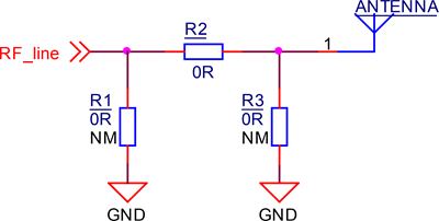
Finding appropriate values for the components should be considered an iterative task. Silicon Labs recommends adding a pi network for matching as shown in the figure below. The following matching strategy is proposed:
Calibrate your Vector Network Analyzer (VNA) for a frequency range larger than the intended bandwidth of the antenna.
Connect an RF coaxial cable to the RF line (for instance, by soldering a pigtail to the line). Connect the RF coaxial cable to a VNA to measure the reflection coefficient, S11, looking into the antenna through the matching network.
Be sure to have a good connection to the ground plane to get the best electrical performance and the highest mechanical robustness during the measurement.
Make sure to route the pigtail towards the center of the PCB and then perpendicularly away from the PCB at the center point. This will limit the effect of the cable on the measured data as much as possible.
Start out with no components on the antenna network shown in the figure below:
The shunt components are not mounted.
The series component is not mounted.
Use line extension on the VNA to move the reference point to the footprint of R1 and R2.
This is achieved when the locus of the S-parameters in the Smith chart on the VNA have assembled in a point at the right edge of the Smith chart.
Mount a 0 resistor at R2 in the figure below.
Measure reflection coefficient for the frequency of interest (the frequency halfway between the lowest frequency and the highest frequency of the region of interest).
Use an online matching tool to calculate series and shunt component values to achieve 50 match on the coaxial line.
This will give a good starting point and should result in a reasonably good match at first attempt.
Iteratively change component values until match is acceptable.
The standard matching criterion is either -6 dB or -10 dB reflection across all frequencies of interest.
When this goal is achieved, Silicon Labs recommends using the same values on a small sample of boards to make sure that the matching is acceptable across production tolerances.
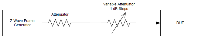
Measurement Setup#
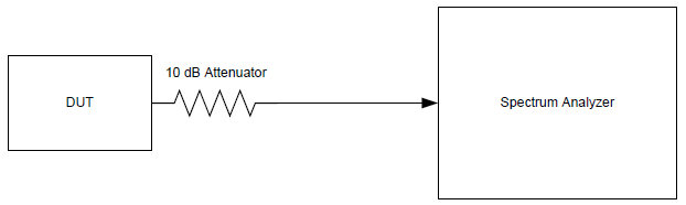
The output power should be measured with a spectrum analyzer as shown in the figure below, and sensitivity should be measured in the following figure. In both cases, place the fixed attenuator as close as possible to the transmitter. The fixed attenuator prevents RF reflections in the measurement setup.
When measuring the sensitivity, first measure and record the output power of the Z-Wave frame generator using the spectrum analyzer. A Z-Wave 800 module programmed with the RAILtest tool can be used as the Z-Wave frame generator. Then, a fixed attenuator can be used along with a variable attenuator to adjust the input power of the DUT. For example, by setting the output power of the Z-Wave generator to -20 dBm, a fixed 50 dB attenuator and a variable 50 dB attenuator can be used to measure the sensitivity with a 1 dB resolution. Place the fixed attenuator close to the Z-Wave generator and conduct the measurements in a radio silent environment, e.g., by placing the DUT in an RF shielded box.