Flash Memory#
A Flash memory is a non-volatile storage device that retains data even after the power is turned off, however, it may need power during the storage process.
Based on the SiWG917 package configuration (OPN), the SiWG917 can have 4 MB or 8 MB of "In-package" or "Stacked" Quad SPI flash. In addition, SiWG917 supports external flash options (up to 16 MB). Quad SPI or QSPI is the interface to access Flash.
Note: Contact Silicon Labs Sales for information about external flash 16MB support.
QSPI Secondary | In-Package Flash Size | External Flash Package Max Size |
|---|---|---|
Flash | 4 MB or 8 MB | 16 MB |
Features:
The first 68 KB is reserved in In-package flash.
The page size is 256 bytes. Flash program command is executed based on a byte or page (256 bytes).
Flash erase is executed based on a sector (4 K-byte) or a 32 KB block (32 K-byte), or a whole chip.
SiWG917 Flash Mode is a common flash device. Single flash is used for both the NWP and M4 processors.
The following are the SiWG917 available OPNs and the possible flash modes.
| Part Number | Flash Size |
|---|---|
| SiWG917M110LGTBA | 4 MB In-package Flash |
| SiWG917M100MGTBA | 8 MB In-package Flash |
| SiWG917M111MGTBA | 8 MB In-package Flash |
| SiWG917M121XGTBA | No Stacked Flash |
| SiWG917M141XGTBA | No Stacked Flash |
| SiWG917M111XGTBA | No Stacked Flash |
Note: Refer to UG574: SiWx917 SoC Manufacturing Utility User Guide for steps on how to select common-flash or dual-flash mode in a No Stacked Flash OPN.
Common Flash#
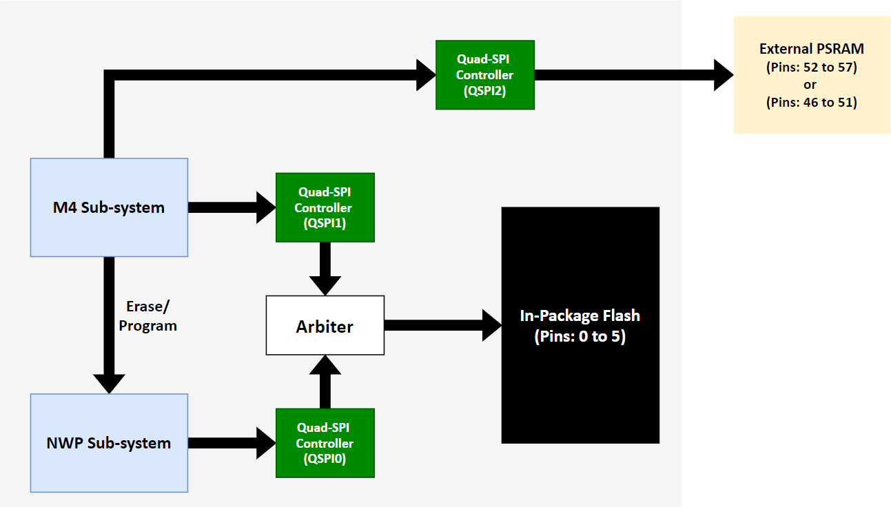
In this flash mode, a single flash memory is shared between M4 and NWP. The two processors access flash memory over dedicated Quad-SPI (QSPI) with an arbiter in between that helps in arbitration for flash accesses.
Though the flash memory is shared between M4 and NWP, only NWP performs low-level flash write operations while M4 supports only flash read operation on the flash memory. For operations such as erasing and writing, M4 requests NWP through a command and sends the data for the write or erase operation.
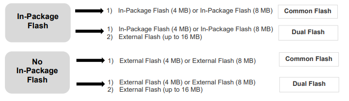
The available flash options are:
In-Package Flash OPN:
In-Package Flash (4 MB)
In-Package Flash (8 MB)
No In-Package Flash OPN:
External Flash (4 MB)
External Flash (8 MB)
Access Diagram (In-Package Flash)#

Access Diagram (No In-Package Flash)#
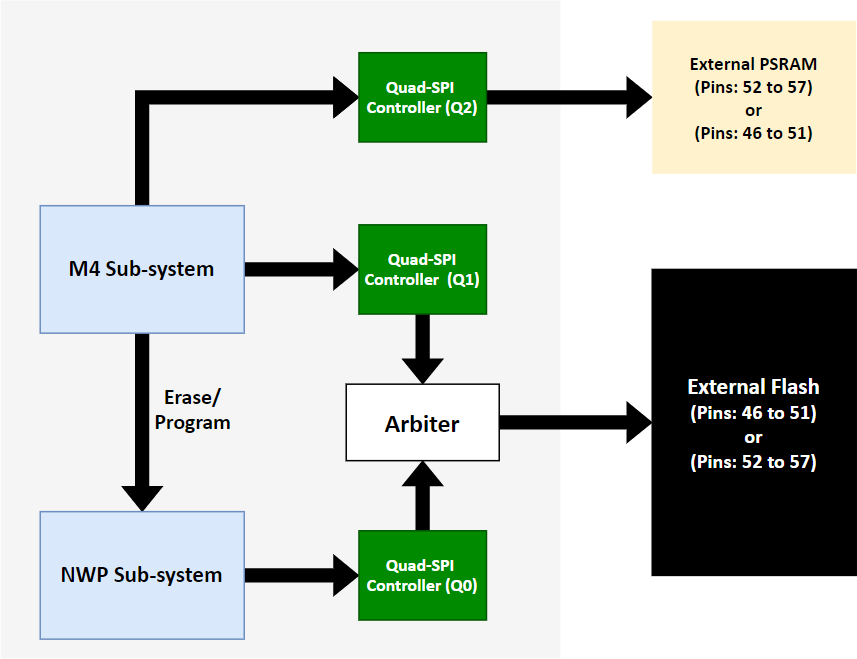
Note: By default, External PSRAM is on Pins: (52 to 57). To configure it to Pins: (46 to 51), refer to the UG574: SiWx917 SoC Manufacturing Utility User Guide.
Memory Map (4 MB)#
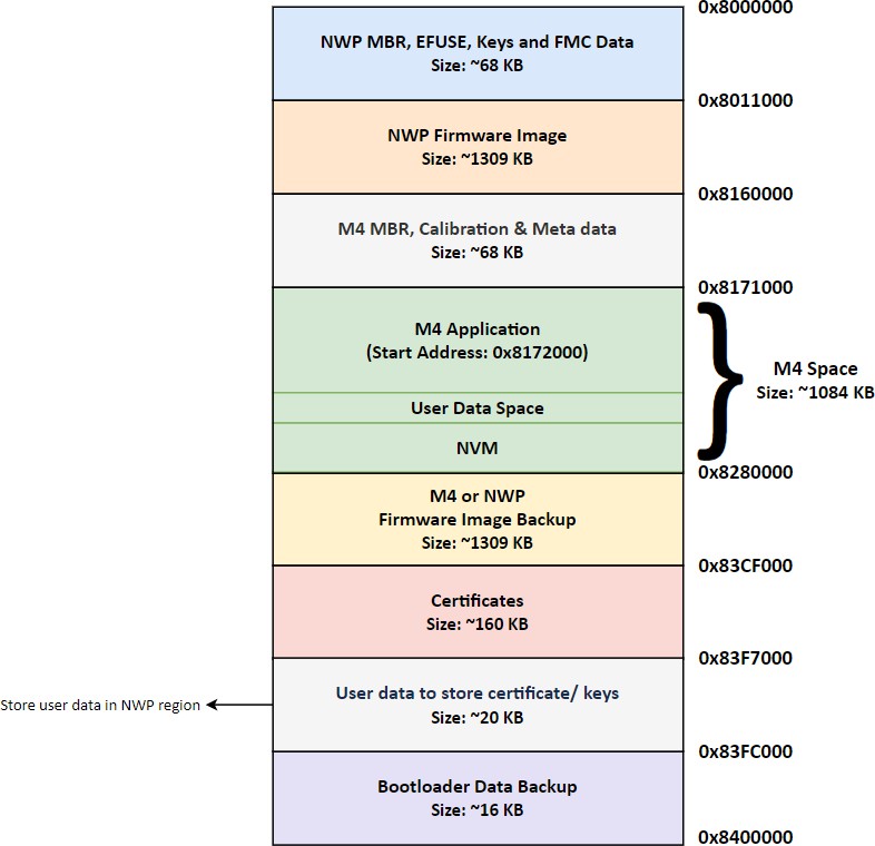
| Component | Size | Application Start Address | |
|---|---|---|---|
M4 Space | M4 Application | Depends on the size of the application | 0x8172000 (Application Execution Start address) |
User Data Space | M4 Space – (M4 Application Size + NVM Size) | 0x8171000 + M4 Application Size | |
NVM | User Configured Size | End of the M4 Space (Depends on back up image size) – NVM Size |
Note: In the linker file, the application execution start address 0x8172000 will be mentioned as the ORIGIN address.
Memory Map (8 MB)#
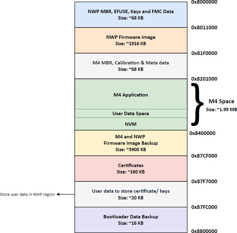
| Component | Size | Application Start Address | |
|---|---|---|---|
M4 Space | M4 Application | Depends on the size of the application | 0x8202000 (Application Execution Start address) |
User Data Space | M4 Space – (M4 Application Size + NVM Size) | 0x8201000 + M4 Application Size + Reserved (alignment) | |
NVM | User Configured Size | End of the M4 Space (Depends on back up image size) – NVM Size |
Note: In the linker file, the application execution start address 0x8202000 will be mentioned as the ORIGIN address.